
Specifications

110 SAM0023-122898 ESS Technology, Inc.
ES1869 DATA SHEET
APPENDIX H: LAYOUT GUIDELINES
APPENDIX H: LAYOUT GUIDELINES
PCB Layout
Notebook, motherboard, pen-based, and PDA portable
computers have the following similarity in PCB layout
design:
1. Multi-layer (usually 4 to 8 layer).
2. Double-sided SMT.
3. CPU, corelogic (chip set), system memory, VGA
controller, and video memory reside in the same
PCB.
This is a very noisy environment for adding an audio
circuit. The following are the guidelines for PCB layout for
an ESS AudioDrive
®
chip application.
Component Placement
The audio circuit-related components, including the audio
I/O jack and connector, must be grouped in the same area.
There are two possible placements for these audio
components:
A grouped on one side of the PCB.
B separated on both sides of the PCB.
In Case B, audio component grouping will take less space.
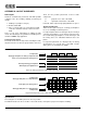
Analog Ground Plane
Audio circuits require two layers of analog ground planes
for use as shielding for all analog traces.
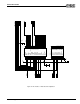
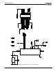
In component placement case A (Figure 47), the first layer
of analog ground plane is on the analog component side,
the second analog ground plane is on the inner layer, and
the analog traces are embedded between these two
planes.
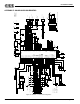
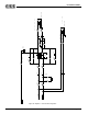
In component placement case B (Figure 48), the analog
ground planes are on both sides of the PCB, and the
analog traces are shielded in the middle.
Case A:
Figure 47 Analog Components on One Side of the PCB
Case B:
Figure 48 Analog Components on Both Sides of the PCB
Special Notes
The analog traces should be placed as short as possible.
The MIC-IN circuit is the most sensitive of the audio circuits, and requires proper and complete shielding.
Analog ground plane on analog component side
Inner one or two layer(s) for analog traces
Inner layer analog ground plane
Other layer(s) for digital traces
Components
Analog ground plane on component side
Inner layer(s) for analog traces
Analog ground plane on component side
Components
Components