
Data Sheet

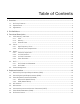
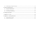

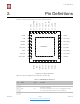
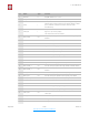
Table Of Contents
- Overview
- Wi-Fi Key Features
- Specifications
- Applications
- CPU, Memory, and Flash
- Clock
- Radio
- Wi-Fi
- Power Management
- General Purpose Input/Output Interface (GPIO)
- Secure Digital Input/Output Interface (SDIO)
- Serial Peripheral Interface (SPI/HSPI)
- I2C Interface
- I2S Interface
- Universal Asynchronous Receiver Transmitter (UART)
- Pulse-Width Modulation (PWM)
- IR Remote Control
- ADC (Analog-to-Digital Converter)
- Electrical Characteristics
- RF Power Consumption
- Wi-Fi Radio Characteristics
- Must-Read Documents
- Must-Have Resources

$
2. Pin Definitions
2. Pin Definitions
Figure 2-1 shows the pin layout for 32-pin QFN package.
$
Figure 2-1. Pin Layout (Top View)
Table 2-1 lists the definitions and functions of each pin.
8
7
6
5
4
3
2
1
X
PD_DCDC
CHIP_EN
TOUT
VDD_RTC
VDD3P3
VDD3P3
LNA
VDDA
17
18
19
20
21
22
23
24 GPIO5
25
26
27
28
29
30
31
32
U0RXD
U0TXD
XTAL_OUT
XTAL_IN
VDDA
RES12K
EXT_RSTB
GPIO4
GPIO0
16
15
14
13
12
11
10
9
GPIO2
MTDO
MTCK
VDDPST
MTDI
MTMS
ESP8266EX
SD_DATA_2
SD_DATA_3
SD_CMD
SD_CLK
SD_DATA_0
SD_DATA_1
VDDD
VDDPST
33 GND
Table 2-1. ESP8266EX Pin Definitions
Pin
Name
Type
Function
1
VDDA
P
Analog Power 2.5 V ~ 3.6 V
2
LNA
I/O
RF antenna interface
Chip output impedance = 39 + j6 Ω. It is suggested to retain
the π-type matching network to match the antenna.
3
VDD3P3
P
Amplifier Power 2.5 V ~ 3.6 V
Espressif
$ /$ 4 26
Submit Documentation Feedback
2020.10