
Data Sheet
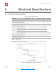
Table Of Contents
- Overview
- Wi-Fi Key Features
- Specifications
- Applications
- CPU, Memory, and Flash
- Clock
- Radio
- Wi-Fi
- Power Management
- General Purpose Input/Output Interface (GPIO)
- Secure Digital Input/Output Interface (SDIO)
- Serial Peripheral Interface (SPI/HSPI)
- I2C Interface
- I2S Interface
- Universal Asynchronous Receiver Transmitter (UART)
- Pulse-Width Modulation (PWM)
- IR Remote Control
- ADC (Analog-to-Digital Converter)
- Electrical Characteristics
- RF Power Consumption
- Wi-Fi Radio Characteristics
- Must-Read Documents
- Must-Have Resources

$
4. Peripheral Interface
Hardware Design
The input voltage range is 0 to 1.0 V when TOUT is connected to external circuit.
RF Initialization
Parameter
The value of the 107th byte of esp_init_data_default.bin (0 ~ 127 bytes),
vdd33_const must be set to the real power supply voltage of Pin3 and Pin4.
The unit and effective value range of vdd33_const is 0.1 V and 18 to 36,
respectively, thus making the working power voltage range of ESP8266EX
between 1.8 V and 3.6 V.
RF Calibration Process
Optimize the RF circuit conditions based on the value of vdd33_const. The
permissible error is ± 0.2 V.
User Programming
Use system_adc_readinstead of system_get_vdd33.
📖 Notes:
esp_init_data_default.bin is provided in SDK package which contains RF initialization parameters (0 ~
127 bytes). The name of the 107th byte in esp_init_data_default.bin is vdd33_const, which is defined as
below:
•
When vdd33_const = 0xff, the power voltage of Pin3 and Pin4 will be tested by the internal self-
calibration process of ESP8266EX itself. RF circuit conditions should be optimized according to the
testing results.
• When 18 = < vdd33_const = < 36, ESP8266EX RF Calibration and optimization process is
implemented via (vdd33_const/10).
• When vdd33_const < 18 or 36 < vdd33_const < 255, vdd33_const is invalid. ESP8266EX RF
Calibration and optimization process is implemented via the default value 3.3 V.
Espressif
$ /$ 18 26
Submit Documentation Feedback
2020.10