
Data Sheet

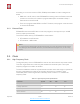

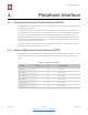

Table Of Contents
- Overview
- Wi-Fi Key Features
- Specifications
- Applications
- CPU, Memory, and Flash
- Clock
- Radio
- Wi-Fi
- Power Management
- General Purpose Input/Output Interface (GPIO)
- Secure Digital Input/Output Interface (SDIO)
- Serial Peripheral Interface (SPI/HSPI)
- I2C Interface
- I2S Interface
- Universal Asynchronous Receiver Transmitter (UART)
- Pulse-Width Modulation (PWM)
- IR Remote Control
- ADC (Analog-to-Digital Converter)
- Electrical Characteristics
- RF Power Consumption
- Wi-Fi Radio Characteristics
- Must-Read Documents
- Must-Have Resources

$
3. Functional Description
3. Functional Description
The functional diagram of ESP8266EX is shown as in Figure 3-1.
$
Figure 3-1. Functional Block Diagram
3.1. CPU, Memory, and Flash
3.1.1. CPU
The ESP8266EX integrates a Tensilica L106 32-bit RISC processor, which achieves extra-
low power consumption and reaches a maximum clock speed of 160 MHz. The Real-Time
Operating System (RTOS) and Wi-Fi stack allow 80% of the processing power to be
available for user application programming and development. The CPU includes the
interfaces as below:
•
Programmable RAM/ROM interfaces (iBus), which can be connected with memory
controller, and can also be used to visit flash.
• Data RAM interface (dBus), which can connected with memory controller.
• AHB interface which can be used to visit the register.
3.1.2. Memory
ESP8266EX Wi-Fi SoC integrates memory controller and memory units including SRAM
and ROM. MCU can access the memory units through iBus, dBus, and AHB interfaces. All
memory units can be accessed upon request, while a memory arbiter will decide the
running sequence according to the time when these requests are received by the
processor.
RF balun
Switch
RF
receive
RF
transmit
Analog
receive
Analog
transmit
PLL VCO 1/2 PLL
Digital baseband
MAC Interface
PMU Crystal Bias circuits SRAM PMU
SDIO
I2C
PWM
ADC
SPI
UART
GPIO
I2S
Flash
Registers
CPU
Sequencers
Accelerator
Espressif
$ /$ 7 26
Submit Documentation Feedback
2020.10