
Data Sheet
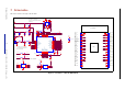
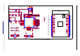
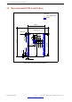
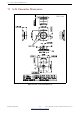
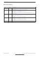
Table Of Contents

8 Peripheral Schematics
8 Peripheral Schematics
This is the typical application circuit of the module connected with peripheral components (for example, power
supply, antenna, reset button, JTAG interface, and UART interface).
5
5
4
4
3
3
2
2
1
1
D
D
C
C
B
B
A
A
IO12 should be kept low when the module is powered on.
EN
SENSOR_VP
SENSOR_VN
IO34
IO35
IO32
IO33
IO25
IO26
IO27
IO14
IO13
IO22
TXD0
RXD0
IO21
IO19
IO18
IO4
IO0
IO5
IO23
IO15
IO2
IO12
ENIO14 TMS
IO12 TDI
IO13 TCK
IO15 TDO
GND
VDD33
GND
VDD33
GND
GND
GND
GND
GND
SW1
R1
TBD
R2 0R
JP2
Boot Option
1
1
2
2
C2
0.1uF
JP1
UART
1
1
2
2
3
3
4
4
JP3
JTAG
1
1
2
2
3
3
4
4
C3
TBD
U1
ESP32-WROVER-E/ESP32-WROVER-IE
GND1
1
3V3
2
EN
3
SENSOR_VP
4
SENSOR_VN
5
IO34
6
IO35
7
IO32
8
IO33
9
IO25
10
IO26
11
IO27
12
IO14
13
IO12
14
GND2
15
IO13
16
NC
17
NC
18
NC
19
NC
20
NC
21
NC
22
IO15
23
IO2
24
IO0
25
IO4
26
NC
27
NC
28
IO5
29
IO18
30
IO19
31
NC
32
IO21
33
RXD0
34
TXD0
35
IO22
36
IO23
37
GND3
38
P_GND
39
C4 0.1uF
C1
22uF
Figure 7: Peripheral Schematics
Note:
• Soldering Pad 39 to the Ground of the base board is not necessary for a satisfactory thermal performance. If users
do want to solder it, they need to ensure that the correct quantity of soldering paste is applied.
• To ensure the power supply to the ESP32 chip during power-up, it is advised to add an RC delay circuit at the EN pin.
The recommended setting for the RC delay circuit is usually R = 10 kΩ and C = 1 µF. However, specific parameters
should be adjusted based on the power-up timing of the module and the power-up and reset sequence timing
of the chip. For ESP32’s power-up and reset sequence timing diagram, please refer to Section Power Scheme in
ESP32 Datasheet.
Espressif Systems 17
Submit Documentation Feedback
ESP32-WROVER-E & ESP32-WROVER-IE Datasheet V1.4