
Data Sheet
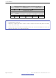
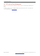
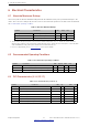
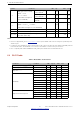
Table Of Contents

6 Electrical Characteristics
Symbol Parameter Min Typ Max Unit
I
OH
High-level source current
(VDD
1
= 3.3 V,
V
OH
>= 2.64 V,
output drive strength set
to the maximum)
VDD3P3_CPU
power domain
1, 2
- 40 - mA
VDD3P3_RTC
power domain
1, 2
- 40 - mA
VDD_SDIO power
domain
1, 3
- 20 - mA
I
OL
Low-level sink current
(VDD
1
= 3.3 V, V
OL
= 0.495 V,
output drive strength set to the maximum)
- 28 - mA
R
P U
Resistance of internal pull-up resistor - 45 - kΩ
R
P D
Resistance of internal pull-down resistor - 45 - kΩ
V
IL_nRST
Low-level input voltage of CHIP_PU
to power off the chip
- - 0.6 V
Notes:
1. Please see Appendix IO_MUX in ESP32 Datasheet for IO’s power domain. VDD is the I/O voltage for a particular power
domain of pins.
2. For VDD3P3_CPU and VDD3P3_RTC power domain, per-pin current sourced in the same domain is gradually reduced
from around 40 mA to around 29 mA, V
OH
>=2.64 V, as the number of current-source pins increases.
3. Pins occupied by flash and/or PSRAM in the VDD_SDIO power domain were excluded from the test.
6.4 WiFi Radio
Table 8: WiFi Radio Characteristics
Parameter Condition Min Typical Max Unit
Operating frequency range
note1
- 2412 - 2484 MHz
Output impedance
note2
- - * - Ω
TX power
note3
11n, MCS7 12 13 14 dBm
11b mode 18.5 19.5 20.5 dBm
Sensitivity
11b, 1 Mbps - –97 - dBm
11b, 11 Mbps - –88 - dBm
11g, 6 Mbps - –92 - dBm
11g, 54 Mbps - –75 - dBm
11n, HT20, MCS0 - –92 - dBm
11n, HT20, MCS7 - –72 - dBm
11n, HT40, MCS0 - –89 - dBm
11n, HT40, MCS7 - –69 - dBm
Adjacent channel rejection
11g, 6 Mbps - 27 - dB
11g, 54 Mbps - 13 - dB
11n, HT20, MCS0 - 27 - dB
11n, HT20, MCS7 - 12 - dB
Espressif Systems 12
Submit Documentation Feedback
ESP32-WROVER-E & ESP32-WROVER-IE Datasheet V1.4