ESP32WROVERE & ESP32WROVERIE Datasheet Version 1.4 Espressif Systems Copyright © 2021 www.espressif.
About This Document This document provides the specifications for the ESP32-WROVER-E and ESP32-WROVER-IE modules. Document Updates Please always refer to the latest version on https://www.espressif.com/en/support/download/documents. Revision History For revision history of this document, please refer to the last page. Documentation Change Notification Espressif provides email notifications to keep customers updated on changes to technical documentation. Please subscribe at www.espressif.com/en/subscribe.
Contents 1 Overview 1 2 Block Diagram 3 3 Pin Definitions 4 3.1 Pin Layout 4 3.2 Pin Description 4 3.3 Strapping Pins 6 4 Functional Description 8 4.1 CPU and Internal Memory 8 4.2 External Flash and SRAM 8 4.3 Crystal Oscillators 8 4.4 RTC and Low-Power Management 9 5 Peripherals and Sensors 10 6 Electrical Characteristics 11 6.1 Absolute Maximum Ratings 11 6.2 Recommended Operating Conditions 11 6.3 DC Characteristics (3.3 V, 25 °C) 11 6.
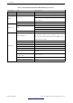
List of Tables 1 Ordering Information 1 2 ESP32-WROVER-E & ESP32-WROVER-IE Specifications 2 3 Pin Definitions 5 4 Strapping Pins 6 5 Absolute Maximum Ratings 11 6 Recommended Operating Conditions 11 7 DC Characteristics (3.
List of Figures 1 ESP32-WROER-E Block Diagram 3 2 ESP32-WROVER-IE Block Diagram 3 3 Pin Layout (Top View) 4 4 Reflow Profile 14 5 Schematics of ESP32-WROVER-E 15 6 Schematics of ESP32-WROVER-IE 16 7 Peripheral Schematics 17 8 Physical Dimensions 18 9 Recommended PCB Land Pattern 19 10 U.
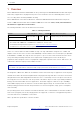
1 Overview 1 Overview ESP32-WROVER-E and ESP32-WROVER-IE are two powerful, generic WiFi-BT-BLE MCU modules that target a wide variety of applications, ranging from low-power sensor networks to the most demanding tasks, such as voice encoding, music streaming and MP3 decoding. ESP32-WROVER-E comes with a PCB antenna, and ESP32-WROVER-IE with an IPEX antenna. They both feature a 4 MB external SPI flash and an additional 8 MB SPI Pseudo static RAM (PSRAM).
1 Overview Table 2: ESP32WROVERE & ESP32WROVERIE Specifications Categories Items Specifications Certification RF certification FCC/CE-RED/SRRC Test Reliablity HTOL/HTSL/uHAST/TCT/ESD 802.11 b/g/n (802.11n up to 150 Mbps) Wi-Fi Protocols A-MPDU and A-MSDU aggregation and 0.4 µs guard interval support Frequency range 2412 ~ 2484 MHz Protocols Bluetooth v4.
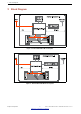
2 Block Diagram 2 Block Diagram ESP32-WROVER-E 40 MHz Crystal 3V3 Antenna RF Matching ESP32-D0WD-V3 GPIOs VDD_SDIO SPICS1 PSRAM_CLK SIO0 SIO1 SIO2 SIO3 VDD_SDIO SPICS0 FLASH_CLK SPIDI SPIDO SPIWP SPIHD SPI PSRAM SPI FLASH EN Figure 1: ESP32WROERE Block Diagram ESP32-WROVER-IE 40 MHz Crystal 3V3 Antenna RF Matching ESP32-D0WD-V3 VDD_SDIO SPICS0 FLASH_CLK SPIDI SPIDO SPIWP SPIHD GPIOs VDD_SDIO SPICS1 PSRAM_CLK SIO0 SIO1 SIO2 SIO3 SPI PSRAM SPI FLASH EN Figure 2: ESP32WROVERIE Block
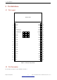
3 Pin Definitions 3 Pin Definitions 3.1 Pin Layout Keepout Zone 1 GND GND 38 2 3V3 IO23 37 3 EN IO22 36 4 SENSOR_VP TXD0 35 5 SENSOR_VN RXD0 34 6 IO34 IO21 33 7 IO35 NC 32 GND GND GND GND Pin 39 GND GND GND GND GND 8 IO32 IO19 31 9 IO33 IO18 30 10 IO25 IO5 29 11 IO26 NC 28 12 IO27 NC 27 13 IO14 IO4 26 14 IO12 IO0 25 15 GND IO2 24 16 IO13 IO15 23 17 NC NC 22 18 NC NC 21 19 NC NC 20 Figure 3: Pin Layout (Top View) 3.
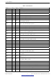
3 Pin Definitions Table 3: Pin Definitions Name No. Type Function GND 1 P Ground 3V3 2 P Power supply EN 3 I Module-enable signal. Active high.
3 Pin Definitions Name No. Type Function RXD0 34 I/O GPIO3, U0RXD, CLK_OUT2 TXD0 35 I/O GPIO1, U0TXD, CLK_OUT3, EMAC_RXD2 IO22 36 I/O GPIO22, VSPIWP, U0RTS, EMAC_TXD1 IO23 37 I/O GPIO23, VSPID, HS1_STROBE GND 38 P Ground Notice: * Pins GPIO6 to GPIO11 on the ESP32-D0WD-V3 chip are connected to the SPI flash integrated on the module and are not led out. 3.
3 Pin Definitions Enabling/Disabling Debugging Log Print over U0TXD During Booting Pin Default U0TXD Active U0TXD Silent MTDO Pull-up 1 0 Timing of SDIO Slave FE Sampling FE Sampling RE Sampling RE Sampling Pin Default FE Output RE Output FE Output RE Output MTDO Pull-up 0 0 1 1 GPIO5 Pull-up 0 1 0 1 Note: • FE: falling-edge, RE: rising-edge.
4 Functional Description 4 Functional Description This chapter describes the modules and functions integrated in ESP32-WROVER-E and ESP32-WROVER-IE. 4.1 CPU and Internal Memory ESP32-D0WD-V3 contains two low-power Xtensa® 32-bit LX6 microprocessors. The internal memory includes: • 448 KB of ROM for booting and core functions. • 520 KB of on-chip SRAM for data and instructions.
4 Functional Description 4.4 RTC and LowPower Management With the use of advanced power-management technologies, ESP32 can switch between different power modes. For details on ESP32’s power consumption in different power modes, please refer to section ”RTC and Low-Power Management” in ESP32 Datasheet. Espressif Systems 9 ESP32-WROVER-E & ESP32-WROVER-IE Datasheet V1.
5 Peripherals and Sensors 5 Peripherals and Sensors Please refer to Section Peripherals and Sensors in ESP32 Datasheet. Note: External connections can be made to any GPIO except for GPIOs in the range 6-11, 16, or 17. GPIOs 6-11 are connected to the module’s integrated SPI flash and PSRAM. GPIOs 16 and 17 are connected to the module’s integrated PSRAM. For details, please see Section 7 Schematics. Espressif Systems 10 ESP32-WROVER-E & ESP32-WROVER-IE Datasheet V1.
6 Electrical Characteristics 6 Electrical Characteristics 6.1 Absolute Maximum Ratings Stresses beyond the absolute maximum ratings listed in the table below may cause permanent damage to the device. These are stress ratings only, and do not refer to the functional operation of the device that should follow the recommended operating conditions. Table 5: Absolute Maximum Ratings Symbol Parameter VDD33 Power supply voltage Ioutput 1 Min Max –0.3 3.
6 Electrical Characteristics Symbol Parameter VDD3P3_CPU High-level source current power domain 1, 1 (VDD = 3.3 V, VDD3P3_RTC VOH >= 2.64 V, IOH 2 power domain 1, output drive strength set 2 VDD_SDIO power to the maximum) domain 1, 3 Min Typ Max Unit - 40 - mA - 40 - mA - 20 - mA - 28 - mA Low-level sink current (VDD1 = 3.3 V, VOL = 0.
6 Electrical Characteristics Notes: 1. Device should operate in the frequency range allocated by regional regulatory authorities. Target operating frequency range is configurable by software. 2. For the modules that use IPEX antennas, the output impedance is 50 Ω. For other modules without IPEX antennas, users do not need to concern about the output impedance. 3. Target TX power is configurable based on device or certification requirements. 6.5 BLE Radio 6.5.
6 Electrical Characteristics Temperature (℃) 6.6 Reflow Profile Peak Temp. 235 ~ 250 ℃ 250 Preheating zone 150 ~ 200 ℃ 60 ~ 120 s 217 200 Reflow zone 217 ℃ 60 ~ 90 s Cooling zone –1 ~ –5 ℃/s Soldering time > 30 s Ramp-up zone 1 ~ 3 ℃/s 100 50 25 Time (sec.) 0 0 50 100 150 200 250 Ramp-up zone — Temp.: 25 ~ 150 ℃ Time: 60 ~ 90 s Ramp-up rate: 1 ~ 3 ℃/s Preheating zone — Temp.: 150 ~ 200 ℃ Time: 60 ~ 120 s Reflow zone — Temp.: >217 ℃ 60 ~ 90 s; Peak Temp.
5 4 3 2 1 7 Schematics This is the reference design of the module. GND The values of C1 and C2 vary with the selection of the crystal. C1 C20 1uF 1 100pF VDD33 GND C9 0 GND GND 2.0nH R1 C5 C13 C11 C10 C21 10uF 1uF 0.1uF NC GPIO21 U0TXD U0RXD GPIO22 GND CAP1 CAP2 VDDA XTAL_P XTAL_N VDDA GPIO21 U0TXD U0RXD GPIO22 49 GND 3 2 499 GND GND 0(NC) ANT2 R14 3 R3 3.3nF/6.3V(10%) J39 IPEX(NC) VDD33 C4 VDD33 D1 LESD8D3.3CAT5G 0.
7 Schematics C20 100pF 1uF VDD33 GND C9 GND 2.0nH R1 C5 C11 C10 C21 10uF 1uF 0.1uF NC 499 GPIO21 U0TXD U0RXD GPIO22 GND GND 0 J39 GND CAP1 CAP2 VDDA XTAL_P XTAL_N VDDA GPIO21 U0TXD U0RXD GPIO22 49 ANT2 R14 3 R3 3.3nF/6.3V(10%) GND 3 2 1 20K(5%) C6 10nF/6.3V(10%) GND 40MHz(±10ppm) 48 47 46 45 44 43 42 41 40 39 L5 0 GND C13 PCB ANTENNA GND R2 0.
8 Peripheral Schematics 8 Peripheral Schematics This is the typical application circuit of the module connected with peripheral components (for example, power supply, antenna, reset button, JTAG interface, and UART interface). U1 C2 R1 22uF 0.
9 Physical Dimensions Espressif Systems 9 Physical Dimensions Unit: mm 18.00±0.15 3.30±0.15 0.85 0.1 0.50 15.84 0.90 10.50 0.57 1.10 0.85 Top View Side View Figure 8: Physical Dimensions Bottom View 16.16 0.50 23.05 24.09 3.70 3.72 0.90 3.70 10.45 1.27 ESP32-WROVER-E & ESP32-WROVER-IE Datasheet V1.4 31.40±0.15 6.22 0.90 6.22 0.45 18 Submit Documentation Feedback 0.80 2.
10 Recommended PCB Land Pattern 10 Recommended PCB Land Pattern Unit: mm Via for thermal pad Copper 6.22 18.00 Antenna Area 38x1.50 3.70 0.90 0.50 0.50 0.90 3.70 16.16 1.27 1.10 7.50 38 22.86 31.40 38x0.90 1 20 19 0.50 Figure 9: Recommended PCB Land Pattern Espressif Systems 19 ESP32-WROVER-E & ESP32-WROVER-IE Datasheet V1.
11 U.FL Connector Dimensions 11 U.FL Connector Dimensions Unit: mm Figure 10: U.FL Connector Dimensions Espressif Systems 20 ESP32-WROVER-E & ESP32-WROVER-IE Datasheet V1.
12 Learning Resources 12 Learning Resources 12.1 MustRead Documents The following link provides documents related to ESP32. • ESP32 Datasheet This document provides an introduction to the specifications of the ESP32 hardware, including overview, pin definitions, functional description, peripheral interface, electrical characteristics, etc. • ESP32 ECO V3 User Guide This document describes differences between V3 and previous ESP32 silicon wafer revisions.
12 Learning Resources • ESP-IDF This webpage links users to the official IoT development framework for ESP32. • ESP32 Resources This webpage provides the links to all available ESP32 documents, SDK and tools. Espressif Systems 22 ESP32-WROVER-E & ESP32-WROVER-IE Datasheet V1.
Revision History Revision History Date Version 2021-02-09 V1.4 Release notes Updated Figure 8: Physical Dimensions Updated Figure 9: Recommended PCB Land Pattern Updated the trade mark from TWAI™ to TWAI® 2021-02-02 V1.3 Modified the note below Figure 4: Reflow Profile Deleted Reset Circuit and Discharge Circuit for VDD33 Rail in Section 8: Peripheral Schematics Updated Figure 3.1: Pin Layout 2020-11-02 V1.
Disclaimer and Copyright Notice Information in this document, including URL references, is subject to change without notice. ALL THIRD PARTY’S INFORMATION IN THIS DOCUMENT IS PROVIDED AS IS WITH NO WARRANTIES TO ITS AUTHENTICITY AND ACCURACY. NO WARRANTY IS PROVIDED TO THIS DOCUMENT FOR ITS MERCHANTABILITY, NONINFRINGEMENT, FITNESS FOR ANY PARTICULAR PURPOSE, NOR DOES ANY WARRANTY OTHERWISE ARISING OUT OF ANY PROPOSAL, SPECIFICATION OR SAMPLE.