ESP32WROOM32E & ESP32WROOM32UE Datasheet Version 1.2 Espressif Systems Copyright © 2021 www.espressif.
About This Document This document provides the specifications for the ESP32-WROOM-32E and ESP32-WROOM-32UE modules. Document Updates Please always refer to the latest version on https://www.espressif.com/en/support/download/documents. Revision History For revision history of this document, please refer to the last page. Documentation Change Notification Espressif provides email notifications to keep customers updated on changes to technical documentation. Please subscribe at www.espressif.
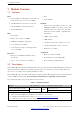
1 Module Overview 1 Module Overview 1.1 Features • AFH MCU ® • ESP32-D0WD-V3 embedded, Xtensa dual-core • CVSD and SBC 32-bit LX6 microprocessor, up to 240 MHz Hardware • 448 KB ROM for booting and core functions • Interfaces: SD card, UART, SPI, SDIO, I2 C, LED • 520 KB SRAM for data and instructions PWM, Motor PWM, I2 S, IR, pulse counter, GPIO, • 16 KB SRAM in RTC capacitive touch sensor, ADC, DAC, Two-Wire Automotive Interface (TWAI® , compatible with WiFi ISO11898-1) • 802.
1 Module Overview At the core of the module is the ESP32-D0WD-V3 chip*. The chip embedded is designed to be scalable and adaptive. There are two CPU cores that can be individually controlled, and the CPU clock frequency is adjustable from 80 MHz to 240 MHz. The chip also has a low-power co-processor that can be used instead of the CPU to save power while performing tasks that do not require much computing power, such as monitoring of peripherals.
Contents Contents 1 Module Overview 3 1.1 Features 3 1.2 Description 3 1.3 Applications 4 2 Block Diagram 9 3 Pin Definitions 10 3.1 Pin Layout 10 3.2 Pin Description 10 3.3 Strapping Pins 12 4 Electrical Characteristics 14 4.1 Absolute Maximum Ratings 14 4.2 Recommended Operating Conditions 14 4.3 DC Characteristics (3.3 V, 25 °C) 14 4.4 Current Consumption Characteristics 15 4.4.1 15 4.5 4.6 4.
Contents 8.3 Reflow Profile 30 9 MAC Addresses and eFuse 31 10 Learning Resources 32 10.1 Must-Read Documents 32 10.2 Must-Have Resources 32 Revision History Espressif Systems 34 6 ESP32-WROOM-32E & ESP32-WROOM-32UE Datasheet v1.
List of Tables List of Tables 1 Ordering Information 2 Pin Definitions 11 3 Strapping Pins 12 4 Absolute Maximum Ratings 14 5 Recommended Operating Conditions 14 6 DC Characteristics (3.
List of Figures List of Figures 1 ESP32-WROOM-32E Block Diagram 9 2 ESP32-WROOM-32UE Block Diagram 9 3 Pin Layout of ESP32-WROOM-32E (Top View) 10 4 ESP32-WROOM-32E Schematics 22 5 ESP32-WROOM-32UE Schematics 23 6 ESP32-WROOM-32E & ESP32-WROOM-32UE Peripheral Schematics 24 7 ESP32-WROOM-32E Physical Dimensions 25 8 ESP32-WROOM-32UE Physical Dimensions 26 9 ESP32-WROOM-32E Recommended PCB Land Pattern 27 10 ESP32-WROOM-32UE Recommended PCB Land Pattern 28 11 U.
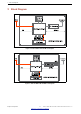
2 Block Diagram 2 Block Diagram 40 MHz Crystal 3V3 Antenna RF Matching ESP32-D0WD-V3 GPIOs SPICS SPICLK SPIDI SPIDO SPIHD SPIWP VDD_SDIO EN SPI Flash ESP32-WROOM-32E Figure 1: ESP32WROOM32E Block Diagram 40 MHz Crystal 3V3 Antenna IPEX RF Matching ESP32-D0WD-V3 GPIOs SPICS SPICLK SPIDI SPIDO SPIHD SPIWP VDD_SDIO EN ESP32-WROOM-32UE SPI Flash Figure 2: ESP32WROOM32UE Block Diagram Espressif Systems 9 ESP32-WROOM-32E & ESP32-WROOM-32UE Datasheet v1.
3 Pin Definitions 3 Pin Definitions 3.
3 Pin Definitions Table 2: Pin Definitions Name No. Type Function GND 1 P Ground 3V3 2 P Power supply EN 3 I High: On; enables the chip Low: Off; the chip powers off Note: Do not leave the pin floating.
3 Pin Definitions Name No. Type Function NC 32 - - IO21 33 I/O GPIO21, VSPIHD, EMAC_TX_EN RXD0 34 I/O GPIO3, U0RXD, CLK_OUT2 TXD0 35 I/O GPIO1, U0TXD, CLK_OUT3, EMAC_RXD2 IO22 36 I/O GPIO22, VSPIWP, U0RTS, EMAC_TXD1 IO23 37 I/O GPIO23, VSPID, HS1_STROBE GND 38 P Ground Note: 1. Pins GPIO6 to GPIO11 on the ESP32-D0WD-V3 chip are connected to the SPI flash integrated on the module and are not led out. 2. For peripheral pin configurations, please refer to ESP32 Datasheet. 3.
3 Pin Definitions Booting Mode Pin Default SPI Boot Download Boot GPIO0 Pull-up 1 0 GPIO2 Pull-down Don’t-care 0 Enabling/Disabling Debugging Log Print over U0TXD During Booting Pin Default U0TXD Active U0TXD Silent MTDO Pull-up 1 0 Timing of SDIO Slave FE Sampling FE Sampling RE Sampling RE Sampling Pin Default FE Output RE Output FE Output RE Output MTDO Pull-up 0 0 1 1 GPIO5 Pull-up 0 1 0 1 Note: • FE: falling-edge, RE: rising-edge.
4 Electrical Characteristics 4 Electrical Characteristics 4.1 Absolute Maximum Ratings Stresses beyond the absolute maximum ratings listed in the table below may cause permanent damage to the device. These are stress ratings only, and do not refer to the functional operation of the device that should follow the recommended operating conditions. Table 4: Absolute Maximum Ratings Symbol Parameter Min Max VDD33 TST ORE Unit Power supply voltage –0.3 3.
4 Electrical Characteristics Symbol Parameter High-level source current 1 (VDD = 3.3 V, IOH Min Typ Max Unit - 40 - mA - 40 - mA - 20 - mA - 28 - mA VDD3P3_CPU power domain 1, 2 VDD3P3_RTC VOH >= 2.64 V, output drive strength set to the maximum) power domain 1, 2 VDD_SDIO power domain 1, 3 Low-level sink current IOL (VDD1 = 3.3 V, VOL = 0.
4 Electrical Characteristics Note: • The current consumption measurements are taken with a 3.3 V supply at 25 °C of ambient temperature at the RF port. All transmitters’ measurements are based on a 50% duty cycle. • The current consumption figures for in RX mode are for cases when the peripherals are disabled and the CPU idle. 4.5 WiFi RF Characteristics 4.5.
4 Electrical Characteristics 4.5.3 Receiver Characteristics Table 10: Receiver Characteristics Parameter RX Sensitivity RX Maximum Input Level Adjacent Channel Rejection Espressif Systems Rate Typ 1 Mbps –97 2 Mbps –94 5.
4 Electrical Characteristics Parameter Rate Typ 11n, HT40, MCS0 16 11n, HT40, MCS7 7 Unit 4.6 Bluetooth Radio 4.6.1 Receiver – Basic Data Rate Table 11: Receiver Characteristics – Basic Data Rate Parameter Conditions Min Typ Max Unit Sensitivity @0.1% BER - –90 –89 –88 dBm Maximum received signal @0.
4 Electrical Characteristics Note: There are a total of eight power levels from 0 to 7, and the transmit power ranges from –12 dBm to 9 dBm. When the power level rises by 1, the transmit power increases by 3 dB. Power level 4 is used by default and the corresponding transmit power is 0 dBm. 4.6.3 Receiver – Enhanced Data Rate Table 13: Receiver Characteristics – Enhanced Data Rate Parameter Conditions Min Typ Max Unit π/4 DQPSK Sensitivity @0.
4 Electrical Characteristics Parameter Conditions π/4 DQPSK modulation accuracy 8 DPSK modulation accuracy In-band spurious emissions EDR differential phase coding Min Typ Max Unit RMS DEVM - 4.28 - % 99% DEVM - 100 - % Peak DEVM - 13.3 - % RMS DEVM - 5.8 - % 99% DEVM - 100 - % Peak DEVM - 14 - % F = F0 ± 1 MHz - –46 - dBm F = F0 ± 2 MHz - –44 - dBm F = F0 ± 3 MHz - –49 - dBm F = F0 +/– > 3 MHz - - –53 dBm - - 100 - % 4.
4 Electrical Characteristics Parameter Min Typ Max F = F0 ± > 3 MHz - –59 - ∆ f 1avg - - - 265 kHz ∆ f 2max - 210 - - kHz ∆ f 2avg /∆ f 1avg - - +0.92 - - ICFT - - –10 - kHz Drift rate - - 0.7 - kHz/50 µs Drift - - 2 - kHz Espressif Systems Conditions 21 Unit dBm ESP32-WROOM-32E & ESP32-WROOM-32UE Datasheet v1.
5 Schematics 5 Schematics This is the reference design of the module. 1uF VDD33 GND R1 C5 GND 20K(5%) 3 TBD VDD33 GND 40MHz(±10ppm) C6 10nF/6.3V(10%) 3.3nF/6.3V(10%) R3 499 C9 0.1uF GPIO21 U0TXD U0RXD GPIO22 D1 LESD8D3.3CAT5G GND C10 C21 10uF NC 1uF 0.1uF NC 49 GND CAP1 CAP2 VDDA XTAL_P XTAL_N VDDA GPIO21 U0TXD U0RXD GPIO22 C11 GND C12 C4 GND VDD33 0.1uF GND GND NC C17 NC The values of C15, L4 and C14 vary with the actual PCB board. NC: No component.
D GND R1 C5 GND 20K(5%) 3 VDD33 1 GND 40MHz(±10ppm) C6 10nF/6.3V(10%) 3.3nF/6.3V(10%) R3 499 C9 0.1uF GPIO21 U0TXD U0RXD GPIO22 D1 LESD8D3.3CAT5G GND C13 C11 C10 C21 10uF 1uF 0.1uF NC GND C GND CAP1 CAP2 VDDA XTAL_P XTAL_N VDDA GPIO21 U0TXD U0RXD GPIO22 49 L5 GND 2.0nH 48 47 46 45 44 43 42 41 40 39 VDD33 C4 GND VDD33 0.
6 Peripheral Schematics 5 4 3 6 Peripheral Schematics This is the typical application circuit of the module connected with peripheral components (for example, power supply, antenna, reset button, JTAG interface, and UART interface). ESP32-WROOM-32E/ESP32-WROOM-32UE 39 P_GND 38 1 GND3 37 2 GND1 IO23 36 3 3V3 IO22 35 4 EN TXD0 34 5 SENSOR_VP RXD0 33 6 SENSOR_VN IO34 IO21 32 7 NC 31 8 IO35 IO19 30 9 IO32 IO18 29 10 IO33 IO5 28 11 IO25 IO17 27 12 IO26 IO16 26 13 IO27 IO4 25 14 IO14 IO12 IO0 VDD33 22uF 0.
7 Physical Dimensions and PCB Layout 7 Physical Dimensions and PCB Layout 7.1 Physical Dimensions Unit: mm 0.85 0.80 0.90 10.50 10.29 0 0.50 0.90 1.27 1.50 15.80 Ø0.5 0.50 3.70 0.1 17.60 0.90 3.70 16.51 25.50±0.15 0.45 6.19 6.19 3.10±0.15 1.05 0.85 8.89 11.43 18.00±0.15 Top View Side View Bottom View Figure 7: ESP32WROOM32E Physical Dimensions Espressif Systems 25 ESP32-WROOM-32E & ESP32-WROOM-32UE Datasheet v1.
7 Physical Dimensions and PCB Layout 3.07 Unit: mm 0.45 3.20±0.15 3.27 0.85 0.80 0.90 10.50 1.18 10.67 0.50 0.90 13.05 1.15 1.27 8.89 0.50 3.70 0.1 16.51 17.50 0.90 3.70 15.65 1.50 19.20±0.15 10.75 0.85 11.43 18.00±0.15 Top View Side View Bottom View Figure 8: ESP32WROOM32UE Physical Dimensions Espressif Systems 26 ESP32-WROOM-32E & ESP32-WROOM-32UE Datasheet v1.
7 Physical Dimensions and PCB Layout 7.2 Recommended PCB Land Pattern Unit: mm Via for thermal pad Copper 6.19 18.00 Antenna Area 38x1.50 3.70 0.90 0.50 16.51 14 15 0.50 1.50 7.50 38 10.29 0.50 0.90 3.70 1.27 1.50 25.50 38x0.90 1 24 25 1.27 0.50 11.43 3.28 Figure 9: ESP32WROOM32E Recommended PCB Land Pattern Espressif Systems 27 ESP32-WROOM-32E & ESP32-WROOM-32UE Datasheet v1.
7 Physical Dimensions and PCB Layout Unit: mm Via for thermal pad Copper 18.00 38x1.50 3.70 0.90 0.50 16.51 14 15 0.50 1.50 7.50 38 10.67 0.50 0.90 3.70 1.27 1.50 19.20 38x0.90 1 24 25 1.27 0.50 11.43 3.28 Figure 10: ESP32WROOM32UE Recommended PCB Land Pattern Espressif Systems 28 ESP32-WROOM-32E & ESP32-WROOM-32UE Datasheet v1.
7 Physical Dimensions and PCB Layout 7.3 U.FL Connector Dimensions Unit: mm Figure 11: U.FL Connector Dimensions Espressif Systems 29 ESP32-WROOM-32E & ESP32-WROOM-32UE Datasheet v1.
8 Product Handling 8 Product Handling 8.1 Storage Condition The products sealed in Moisture Barrier Bag (MBB) should be stored in a noncondensing atmospheric environment of < 40 °C/90% RH. The module is rated at moisture sensitivity level (MSL) 3. After unpacking, the module must be soldered within 168 hours with factory conditions 25±5 °C and 60% RH. The module needs to be baked if the above conditions are not met. 8.
9 MAC Addresses and eFuse 9 MAC Addresses and eFuse The eFuse in ESP32 has been burnt into 48-bit mac_address.
10 Learning Resources 10 Learning Resources 10.1 MustRead Documents The following link provides documents related to ESP32. • ESP32 Datasheet This document provides an introduction to the specifications of the ESP32 hardware, including overview, pin definitions, functional description, peripheral interface, electrical characteristics, etc. • ESP32 ECO V3 User Guide This document describes differences between V3 and previous ESP32 silicon wafer revisions.
10 Learning Resources • ESP-IDF This webpage links users to the official IoT development framework for ESP32. • ESP32 Resources This webpage provides the links to all available ESP32 documents, SDK and tools. Espressif Systems 33 ESP32-WROOM-32E & ESP32-WROOM-32UE Datasheet v1.
Revision History Revision History Date Version Release notes Updated Figure 9: ESP32-WROOM-32E Recommended PCB Land Pattern, Figure 10: ESP32-WROOM-32UE Recommended PCB Land Pattern, Figure 7: 2021-02-09 V1.2 ESP32-WROOM-32E Physical Dimensions, and Figure 8: ESP32-WROOM-32UE Physical Dimensions. Modified the note below Figure 12: Reflow Profile. Updated the trade mark from TWAI™ to TWAI® . Updated the table 7. 2020-11-02 V1.1 Added a note to EPAD in Section 7.2 Recommended PCB Land Pattern.
Disclaimer and Copyright Notice Information in this document, including URL references, is subject to change without notice. ALL THIRD PARTY’S INFORMATION IN THIS DOCUMENT IS PROVIDED AS IS WITH NO WARRANTIES TO ITS AUTHENTICITY AND ACCURACY. NO WARRANTY IS PROVIDED TO THIS DOCUMENT FOR ITS MERCHANTABILITY, NONINFRINGEMENT, FITNESS FOR ANY PARTICULAR PURPOSE, NOR DOES ANY WARRANTY OTHERWISE ARISING OUT OF ANY PROPOSAL, SPECIFICATION OR SAMPLE.