
Data Sheet
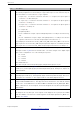
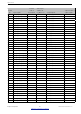
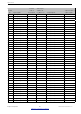
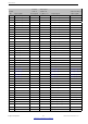
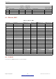
Table Of Contents
- 1 Overview
- 2 Pin Definitions
- 3 Functional Description
- 4 Peripherals and Sensors
- 4.1 Descriptions of Peripherals and Sensors
- 4.1.1 General Purpose Input / Output Interface (GPIO)
- 4.1.2 Analog-to-Digital Converter (ADC)
- 4.1.3 Hall Sensor
- 4.1.4 Digital-to-Analog Converter (DAC)
- 4.1.5 Touch Sensor
- 4.1.6 Ultra-Low-Power Co-processor
- 4.1.7 Ethernet MAC Interface
- 4.1.8 SD/SDIO/MMC Host Controller
- 4.1.9 SDIO/SPI Slave Controller
- 4.1.10 Universal Asynchronous Receiver Transmitter (UART)
- 4.1.11 I²C Interface
- 4.1.12 I²S Interface
- 4.1.13 Infrared Remote Controller
- 4.1.14 Pulse Counter
- 4.1.15 Pulse Width Modulation (PWM)
- 4.1.16 LED PWM
- 4.1.17 Serial Peripheral Interface (SPI)
- 4.1.18 Accelerator
- 4.2 Peripheral Pin Configurations
- 4.1 Descriptions of Peripherals and Sensors
- 5 Electrical Characteristics
- 6 Package Information
- 7 Part Number and Ordering Information
- 8 Learning Resources
- Appendix A – ESP32 Pin Lists
- Revision History

Appendix A
Appendix A – ESP32 Pin Lists
A.1. Notes on ESP32 Pin Lists
Table 24: Notes on ESP32 Pin Lists
No. Description
1
In Table IO_MUX, the boxes highlighted in yellow indicate the GPIO pins that are input-only.
Please see the following note for further details.
2
GPIO pins 34-39 are input-only. These pins do not feature an output driver or internal pull-
up/pull-down circuitry. The pin names are: SENSOR_VP (GPIO36), SENSOR_CAPP (GPIO37),
SENSOR_CAPN (GPIO38), SENSOR_VN (GPIO39), VDET_1 (GPIO34), VDET_2 (GPIO35).
3
The pins are grouped into four power domains: VDDA (analog power supply), VDD3P3_RTC
(RTC power supply), VDD3P3_CPU (power supply of digital IOs and CPU cores), VDD_SDIO
(power supply of SDIO IOs). VDD_SDIO is the output of the internal SDIO-LDO. The voltage of
SDIO-LDO can be configured at 1.8 V or be the same as that of VDD3P3_RTC. The strapping
pin and eFuse bits determine the default voltage of the SDIO-LDO. Software can change the
voltage of the SDIO-LDO by configuring register bits. For details, please see the column “Power
Domain” in Table IO_MUX.
4
The functional pins in the VDD3P3_RTC domain are those with analog functions, including the
32 kHz crystal oscillator, ADC, DAC, and the capacitive touch sensor. Please see columns
“Analog Function 1~3” in Table IO_MUX.
5
These VDD3P3_RTC pins support the RTC function, and can work during Deep-sleep. For
example, an RTC-GPIO can be used for waking up the chip from Deep-sleep.
6
The GPIO pins support up to six digital functions, as shown in columns “Function 1~6” In Table
IO_MUX. The function selection registers will be set as “N-1”, where N is the function number.
Below are some definitions:
• SD_* is for signals of the SDIO slave.
• HS1_* is for Port 1 signals of the SDIO host.
• HS2_* is for Port 2 signals of the SDIO host.
• MT* is for signals of the JTAG.
• U0* is for signals of the UART0 module.
• U1* is for signals of the UART1 module.
• U2* is for signals of the UART2 module.
• SPI* is for signals of the SPI01 module.
• HSPI* is for signals of the SPI2 module.
• VSPI* is for signals of the SPI3 module.
Espressif Systems 51
Submit Documentation Feedback
ESP32 Series Datasheet v3.5