
Data Sheet
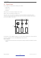
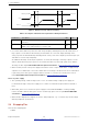
Table Of Contents
- 1 Overview
- 2 Pin Definitions
- 3 Functional Description
- 4 Peripherals and Sensors
- 4.1 Descriptions of Peripherals and Sensors
- 4.1.1 General Purpose Input / Output Interface (GPIO)
- 4.1.2 Analog-to-Digital Converter (ADC)
- 4.1.3 Hall Sensor
- 4.1.4 Digital-to-Analog Converter (DAC)
- 4.1.5 Touch Sensor
- 4.1.6 Ultra-Low-Power Co-processor
- 4.1.7 Ethernet MAC Interface
- 4.1.8 SD/SDIO/MMC Host Controller
- 4.1.9 SDIO/SPI Slave Controller
- 4.1.10 Universal Asynchronous Receiver Transmitter (UART)
- 4.1.11 I²C Interface
- 4.1.12 I²S Interface
- 4.1.13 Infrared Remote Controller
- 4.1.14 Pulse Counter
- 4.1.15 Pulse Width Modulation (PWM)
- 4.1.16 LED PWM
- 4.1.17 Serial Peripheral Interface (SPI)
- 4.1.18 Accelerator
- 4.2 Peripheral Pin Configurations
- 4.1 Descriptions of Peripherals and Sensors
- 5 Electrical Characteristics
- 6 Package Information
- 7 Part Number and Ordering Information
- 8 Learning Resources
- Appendix A – ESP32 Pin Lists
- Revision History

2 Pin Definitions
2.3 Power Scheme
ESP32’s digital pins are divided into three different power domains:
• VDD3P3_RTC
• VDD3P3_CPU
• VDD_SDIO
VDD3P3_RTC is also the input power supply for RTC and CPU.
VDD3P3_CPU is also the input power supply for CPU.
VDD_SDIO connects to the output of an internal LDO whose input is VDD3P3_RTC. When VDD_SDIO is
connected to the same PCB net together with VDD3P3_RTC, the internal LDO is disabled automatically. The
power scheme diagram is shown below:
SDIO
Domain
RTC
Domain
CPU
Domain
LDOLDO LDO1.8 V 1.1 V1.1 V
VDD3P3_RTC VDD3P3_CPU
VDD_SDIO
3.3 V/1.8 V
Figure 4: ESP32 Power Scheme
The internal LDO can be configured as having 1.8 V, or the same voltage as VDD3P3_RTC. It can be powered off
via software to minimize the current of flash/SRAM during the Deep-sleep mode.
Notes on CHIP_PU:
• The illustration below shows the ESP32 power-up and reset timing. Details about the parameters are listed
in Table 2.
Espressif Systems 18
Submit Documentation Feedback
ESP32 Series Datasheet v3.5