
Data Sheet

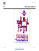
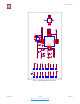


Table Of Contents

!
6. Peripheral Schematics
6. Peripheral Schematics
!
Figure 6-1. ESP-WROOM-02D/ESP-WROOM-02U Peripheral Schematics
EN
IO14
IO12
IO13
IO15
IO2
IO0
IO16
IO5
IO4
ADC
RXD
RST
TXD
VDD33
GND
VDD33
GND
GND
GNDGND
GND
GND
J2
BOOT OPTION
1
2
U1
3V3
1
EN
2
IO14
3
IO12
4
IO13
5
IO15
6
IO2
7
IO0
8
GND1
9
IO4
10
RXD
11
TXD
12
GND2
13
IO5
14
RST
15
TOUT
16
IO16
17
GND3
18
P_GND
19
J1
UART DOWNLOAD
1
2
3
C2 0.1uF
C3 0.1uF
R2 10K
C1 10uF
R1
10K
📖 Note:
1. Soldering Pad 19 to the Ground of the base board is not necessary for a satisfactory thermal
performance. If users do want to solder it, they need to ensure that the correct quantity of soldering paste
is applied.
2. To ensure the power supply to the ESP8266EX chip during the power-up, it is advised to add an RC delay
circuit at the EN pin. The recommended setting for the RC delay circuit is usually R = 10 kΩ and C = 0.1
uF. However, specific parameters should be adjusted based on the power-up timing of the module and
the power-up and reset timing of the ESP8266 chip. For ESP8266EX’s Power-up and Reset Timing
Diagram, please refer to Electrical Characteristics in ESP8266EX Datasheet.
3. To improve module’s anti-inference capability, it is advised to reserve an RC delay circuit at the RST pin.
The recommended setting for the RC delay circuit is usually R= 10 kΩ and C = 0.1 uF.
Espressif
! /! 14 22
Submit Documentation Feedback
2020.07