
User's Manual
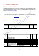
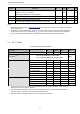
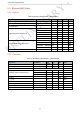
Table Of Contents

5. Electrical Characteristics
Symbol
Parameter
Min
Typ
Max
Unit
Low-level sink current
I
OL
(VDD
1
= 3.3 V, V
OL
= 0.495 V,
-
28
-
mA
output drive strength set to the maximum)
R
P U
Resistance of internal pull-up resistor
-
45
-
kΩ
R
P D
Resistance of internal pull-down resistor
-
45
-
kΩ
V
IL_nRST
Low-level input voltage of CHIP_PU to power off the chip
-
-
0.6
V
Notes:
1. Please see Appendix IO_MUX of ESP32 Datasheet for IO’s power domain. VDD is the I/O voltage for a particular
power domain of pins.
2. For VDD3P3_CPU and VDD3P3_RTC power domain, per-pin current sourced in the same domain is gradually
reduced from around 40 mA to around 29 mA, V
OH
>=2.64 V, as the number of current-source pins increases.
3. Pins occupied by flash and/or PSRAM in the VDD_SDIO power domain were excluded from the test.
5.4 Wi-Fi Radio
Table 8: Wi-Fi Radio Characteristics
Parameter
Condition
Min
Typical
Max
Unit
Operating frequency range
note1
-
2412
-
2462
MHz
TX power
no
te2
dBm
Sensitivity
11b, 1 Mbps
-
–98
-
dBm
11b, 11 Mbps
-
–89
-
dBm
11g, 6 Mbps
-
–92
-
dBm
11g, 54 Mbps
-
–74
-
dBm
11n, HT20, MCS0
-
–91
-
dBm
11n, HT20, MCS7
-
–71
-
dBm
11n, HT40, MCS0
-
–89
-
dBm
11n, HT40, MCS7
-
–69
-
dBm
Adjacent channel rejection
11g, 6 Mbps
-
31
-
dB
11g, 54 Mbps
-
14
-
dB
11n, HT20, MCS0
-
31
-
dB
11n, HT20, MCS7
-
13
-
dB
1. Device should operate in the frequency range allocated by regional regulatory authorities. Target operating
frequency range is configurable by software.
2. For the modules that use IPEX antennas, the output impedance is 50 Ω. For other modules without IPEX
antennas, users do not need to concern about the output impedance.
3. Target TX power is configurable based on device or certification requirements.
11
802.11b:26.62dBm;802.11g:25.91dBm
802.11n20:25.89dBm;802.11n40:26.51dBm