
User's Manual
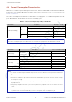
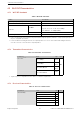
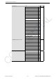

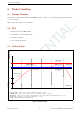

Table Of Contents

CONFIDENTIAL
7. Physical Dimensions and PCB Land Pattern
7. Physical Dimensions and PCB Land Pattern
7.1 Physical Dimensions
31.00
18.00
0.80
3.30
1.50
0.45
0.90
0.85
15.45
10.19
4.00
4.00
2.25
0.45
ESP32-S2-WROVER Dimensions
Unit: mm
Tolerance: +/-0.10mm
Top View
Side View
Bottom View
6.30
8.35
23.10
15.84
19.30
10.44
1.50
1.00
0.50
1.00
0.50
0.85
0.90
0.90
1.00
2.25
Figure 5: ESP32-S2-WROVER Physical Dimensions
Espressif Systems
15
ESP32-S2-WROVER User Manual V0.1
Note:
• Soldering the EPAD to the ground of the base board is not a must, though doing so can get optimized thermal
performance. If users do want to solder it, they need to ensure that the correct quantity of soldering paste is applied.
• To ensure the power supply to the ESP32-S2 chip during power-up, it is advised to add an RC delay circuit at the
EN pin. The recommended setting for the RC delay circuit is usually R = 10 kΩ and C = 0.1 µF. However, specific
parameters should be adjusted based on the power-up timing of the module and the power-up and reset sequence
timing of the chip. For ESP32-S2’s power-up and reset sequence timing diagram, please refer to Section Power
Scheme in ESP32-S2 Datasheet.