
User's Manual
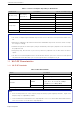
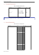
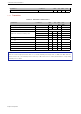
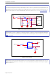
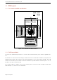
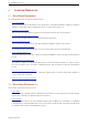
Table Of Contents
- 1 Module Overview
- 3 Pin Definitions
- 4 Electrical Characteristics
- 7 Physical Dimensions and PCB Layout
- 8 Product Handling
- 9 MAC Addresses and eFuse
- 11 Learning Resources
- Revision History
- 空白页面

4.
Peripheral Schematics
Note:
To ensure the power supply to the ESP32 chip during power-up, it is advised to add an RC delay circuit at the EN pin. The
recommended setting for the RC delay circuit is usually R = 10 kΩ and C = 0.1 µF. However, specific parameters should
be adjusted based on the power-up timing of the module and the power-up and reset sequence timing of the chip. For
ESP32’s power-up and reset sequence timing diagram, please refer to Section Power Scheme in ESP32 User Manual.
VCC
GND
GND
GND
VDD33
GND
ESP Modu
le
Discharge
Circuit CAP Added By User
Q1
R1
100K
D1SW1
1 2
R2
1K
+
C1
Bulk CAP
Figure 2: Discharge Circuit for VDD33 Rail
Note:
The discharge circuit can be applied in scenarios where ESP32 is powered on and off repeatedly by switching the
power rails, and there is a large capacitor on the VDD33 rail. For details, please refer to Section Power Scheme in
ESP32 User Manual.
5
5
4
4
3
3
2
2
1
1
D D
C C
B B
A A
CHIP_PU
VBAT
GND
GND
Titl
e
Size
Document Number Rev
D
ate: Sheet o f
<Doc> V1
<ResetCirciut>
A4
1 1Thursday, May 31,
2018
Titl
e
Size
Document Number Rev
D
ate: Sheet o f
<Doc> V1
<ResetCirciut>
A4
1 1Thursday, May 31,
2018
Titl
e
Size
Document Number Rev
D
ate: Sheet o f
<Doc> V1
<ResetCirciut>
A4
1 1Thursday, May 31,
2018
R1 0R
R2
100K
U1
Power Supply Supervisor
GND
1
VCC
3
RESET#
2
Figure 3: Reset Circuit
Note:
When battery is used as the power supply for ESP32 series of chips and modules, a supply voltage supervisor is recom-
mended to avoid boot failure due to low voltage. Users are recommended to pull CHIP_PU low if the power supply for
ESP32 is below 3.0 V.
Espressif Systems