
Service manual


EPSON Stylus Photo 870/1270 Revision B
OPERATING PRINCIPLES Electrical Circuit Operating Principles 49
2.2.2.2 Reset Circuit
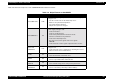
Reset circuits are attached on the C304MAIN board to monitor the two
voltages: +5V for the logic line and +42V for the drive line. When each
circuit detects abnormality on the corresponding line, it resets CPU and
ASIC to prevent the printer from operating abnormally. IC5 RTC-9820SA,
the reset circuit IC attached directly on the main board, monitors both +5V
and +45 lines but can reset them independently. See Figure 2-14 for the
block diagram for the reset circuits.
Figure 2-14. Reset Circuit Block Diagram
"
+5V line reset circuit
The VDD port of IC5 reset IC monitors the +5V line. When the IC
detects an abnormal voltage level (4.3 V or lower), it outputs a reset
signal from the RST port to CPU and ASIC.
"
+42V line reset circuit
The VIN port of the IC5 reset IC monitors the +45V line. When the IC
detects an abnormal voltage level (35.5V or lower), it outputs a reset
signal from the VDT port to CPU and ASIC.
NOTE:
IC5, also serving as RIC (Real Time Clock), manages timer control
when the printer power is turned off. Power for this operation is
supplied from the BAT1.
2.2.2.3 Motor Driver Circuit
The Stylus Photo 870/1270 is equipped with the CR motor and PF motor
that are DC motors and ASF/Pump motor, a stepping motor. To control
the DC motors, a slave CPU is mounted on the C304MAIN board beside
the CPU and ASIC. Since the slave CPU is exclusively used to control DC
motors, it reduces duty of CPU and ASIC to offer faster data processing.
CR motor driver circuit
The internal equivalent circuit of the CR motor driver IC (LB1947) is as
shown below.
Figure 2-15. Internal Equivalent Circuit of the CR Motor Driver IC
The Slave CPU (C90A26CA) controls the CR position by referring to the
pulses sent from the linear encoder via ASIC (IC18). Based on the data
sent from ASIC, the CPU sets an appropriate drive current value used to
VDT
FRST
RST
CE
SCLK
DATA
VIN
VDD
VBK
GND
+42V +5V
NMI
MRES
RESET
C21
0.1U
C19
0.1U
C18
0.1U
TCE
TCLK
TDATA
D2
SB007-03CPTB
IC8
E05B70CD
BAT1
CR2032
+3.3V
R26
3.3K
R27
3.3K
IC18
LB1947
IC15
C90A13CA
IC8
E05B70CD
CR-A
CR-B
OUTA
OUTB
NMI
NMI
P31
RXD1
P33TXD1
P32CRBI3
P30
CRPHAB
P64CRENBB
RES
CRAI2
MD2
P25
CPU
CRBI3
CRAI0
ENA
ENB
CRAI1
CR
E
GND
R115
68BK
R114
12.7K
C117
1500p
R112
0.499
C115
0.1U
+5V
+42V
VBB
IN1
IN2
ST
VI
MD
PE1
PE2
PE0
PE4
PA0
VREF
+
-
IC24
M62552FP
R138
4.4BK
R139
4.99BK
DA1
P12
P26
P11
P13
P27
CRBI2
CN8
HEAD FFC