S1D13705 Embedded Memory LCD Controller S1D13705 TECHNICAL MANUAL Document No. X27A-Q-001-04 Copyright © 2001 Epson Research and Development, Inc. All Rights Reserved. Information in this document is subject to change without notice. You may download and use this document, but only for your own use in evaluating Seiko Epson/EPSON products. You may not modify the document. Epson Research and Development, Inc. disclaims any representation that the contents of this document are accurate or current.
Page 2 Epson Research and Development Vancouver Design Center THIS PAGE LEFT BLANK S1D13705 X27A-Q-001-04 TECHNICAL MANUAL Issue Date: 01/04/18
Epson Research and Development Vancouver Design Center Page 3 Customer Support Information Comprehensive Support Tools Seiko Epson Corp. provides to the system designer and computer OEM manufacturer a complete set of resources and tools for the development of graphics systems. Evaluation / Demonstration Board • Assembled and fully tested graphics evaluation board with installation guide and schematics. • To borrow an evaluation board, please contact your local Seiko Epson Corp. sales representative.
Page 4 Epson Research and Development Vancouver Design Center THIS PAGE LEFT BLANK S1D13705 X27A-Q-001-04 TECHNICAL MANUAL Issue Date: 01/04/18
ENERGY S AV I N G GRAPHICS EPSON S1D13705 February 2001 S1D13705 Embedded Memory LCD Controller The S1D13705 is a color/monochrome LCD graphics controller with an embedded 80K Byte SRAM display buffer. The high integration of the S1D13705 provides a low cost, low power, single chip solution to meet the requirements of embedded markets such as Office Automation equipment, Mobile Communications devices, and Palm-size PCs where board size and battery life are major concerns.
GRAPHICS S1D13705 ■ DESCRIPTION Memory Interface • Display Modes Embedded 80K byte SRAM display buffer. CPU Interface • • Direct support for: Hitachi SH-3. Hitachi SH-4. Motorola M68xxx. MPU bus interface with programmable READY. CPU write buffer. 4/8-bit monochrome LCD interface. 4/8-bit color LCD interface. Single-panel, single-drive passive displays. Dual-panel, dual-drive passive displays. Active matrix TFT / D-TFD interface. Example resolutions: 640x480 at a color depth of 2 bpp.
S1D13705 Embedded Memory LCD Controller Hardware Functional Specification Document Number: X27A-A-001-10 Copyright © 1999, 2002 Epson Research and Development, Inc. All Rights Reserved. Information in this document is subject to change without notice. You may download and use this document, but only for your own use in evaluating Seiko Epson/EPSON products. You may not modify the document. Epson Research and Development, Inc.
Page 2 Epson Research and Development Vancouver Design Center THIS PAGE LEFT BLANK S1D13705 X27A-A-001-10 Hardware Functional Specification Issue Date: 02/02/01
Epson Research and Development Vancouver Design Center Page 3 Table of Contents 1 Introduction . . . . . . . . . . . . . . . . . . . . . . . . . . . . . . . . . . . . . . . . 9 1.1 Scope . . . . . . . . . . . . . . . . . . . . . . . . . . . . . . . . . . . 9 1.2 Overview Description . . . . . . . . . . . . . . . . . . . . . . . . . . . . 9 2 Features . . . . . . . . . . 2.1 Integrated Frame Buffer 2.2 CPU Interface . . . . 2.3 Display Support . . . . 2.4 Display Modes . . . . 2.5 Clock Source . . . . .
Page 4 Epson Research and Development Vancouver Design Center 7.1.5 Generic #1 Interface Timing . . . . . . . . . . . 7.1.6 Generic #2 Interface Timing . . . . . . . . . . . 7.2 Clock Input Requirements . . . . . . . . . . . 7.3 Display Interface . . . . . . . . . . . . . . . 7.3.1 Power On/Reset Timing . . . . . . . . . . . . . 7.3.2 Power Down/Up Timing . . . . . . . . . . . . 7.3.3 Single Monochrome 4-Bit Panel Timing . . . . 7.3.4 Single Monochrome 8-Bit Panel Timing . . . . 7.3.
Epson Research and Development Vancouver Design Center Page 5 List of Tables Table 5-1: Summary of Power On/Reset Options . . . . . . . . . . . . . . . . Table 5-2: Host Bus Interface Pin Mapping . . . . . . . . . . . . . . . . . . . Table 5-3: LCD Interface Pin Mapping . . . . . . . . . . . . . . . . . . . . . Table 6-1: Absolute Maximum Ratings . . . . . . . . . . . . . . . . . . . . . Table 6-2: Recommended Operating Conditions for Core VDD = 3.3V ± 10% Table 6-3: Input Specifications . . . . . . . . .
Page 6 Epson Research and Development Vancouver Design Center THIS PAGE LEFT BLANK S1D13705 X27A-A-001-10 Hardware Functional Specification Issue Date: 02/02/01
Epson Research and Development Vancouver Design Center Page 7 List of Figures Figure 3-1: Figure 3-2: Figure 3-3: Figure 3-4: Figure 3-5: Figure 3-6: Figure 4-1: Figure 5-1: Figure 7-1: Figure 7-2: Figure 7-3: Figure 7-4: Figure 7-5: Figure 7-6: Figure 7-7: Figure 7-8: Figure 7-9: Figure 7-10: Figure 7-11: Figure 7-12: Figure 7-13: Figure 7-14: Figure 7-15: Figure 7-16: Figure 7-17: Figure 7-18: Figure 7-19: Figure 7-20: Figure 7-21: Figure 7-22: Figure 7-23: Figure 7-24: Figure 7-25: Figure 7-26: Figure
Page 8 Figure 11-2: Figure 11-3: Figure 11-4: Figure 11-5: Figure 11-6: Figure 11-7: Figure 12-1: Epson Research and Development Vancouver Design Center 2 Bit-per-pixel Monochrome Mode Data Output Path . . . . . . . . . 4 Bit-per-pixel Monochrome Mode Data Output Path . . . . . . . . . 1 Bit-per-pixel Color Mode Data Output Path . . . . . . . . . . . . . 2 Bit-per-pixel Color Mode Data Output Path . . . . . . . . . . . . . 4 Bit-per-pixel Color Mode Data Output Path . . . . . . . . . . . . .
Epson Research and Development Vancouver Design Center Page 9 1 Introduction 1.1 Scope This is the Hardware Functional Specification for the S1D13705 Embedded Memory LCD Controller Chip. Included in this document are timing diagrams, AC and DC characteristics, register descriptions, and power management descriptions. This document is intended for two audiences: Video Subsystem Designers and Software Developers. This document is updated as appropriate.
Page 10 Epson Research and Development Vancouver Design Center 2 Features 2.1 Integrated Frame Buffer • Embedded 80K byte SRAM display buffer. 2.2 CPU Interface • Direct support of the following interfaces: Hitachi SH-3. Hitachi SH-4. Motorola M68K. MPU bus interface using WAIT# signal. • Direct memory mapping of internal registers. • Single level CPU write buffer. • Registers are mapped into upper 32 bytes of 128K byte address space.
Epson Research and Development Vancouver Design Center Page 11 2.4 Display Modes • SwivelView™: direct 90° hardware rotation of display image for portrait mode display • 1/2/4 bit-per-pixel (bpp), 2/4/16-level grayscale display. • 1/2/4/8 bit-per-pixel, 2/4/16/256-level color display. • Up to 16 shades of gray by FRM on monochrome passive LCD panels; a 256x4 LookUp Table is used to map 1/2/4 bpp modes into these shades.
Page 12 Epson Research and Development Vancouver Design Center 3 Typical System Implementation Diagrams . CLKI Oscillator SH-4 BUS CSn# CS# A[16:0] AB[16:0] D[15:0] DB[15:0] WE1# BS# RD/WR# RD# WE1# BS# FPDAT[7:0] S1D13705 RD/WR# WE0# RDY# WAIT# CKIO BCLK FPSHIFT FPFRAME FPFRAME 8-bit FPLINE RD# WE0# D[7:0] FPSHIFT DRDY FPLINE MOD LCD Display LCDPWR RESET# RESET# Figure 3-1: Typical System Diagram (SH-4 Bus) .
Epson Research and Development Vancouver Design Center Page 13 . Oscillator A[23:17] FC0, FC1, FC2 Decoder CS# A[16:1] AB[16:1] D[15:0] DB[15:0] LDS# AB0 UDS# WE1# AS# CLKI MC68000 BUS FPDAT[7:4] S1D13705 R/W# FPFRAME FPFRAME 4-bit DRDY RD/WR# DTACK# FPSHIFT FPLINE BS# D[3:0] FPSHIFT FPLINE MOD LCD Display WAIT# LCDPWR CLK BCLK RESET# RESET# Figure 3-3: Typical System Diagram (M68K #1 Bus) .
Page 14 Epson Research and Development Vancouver Design Center . CLKI Oscillator BS# GENERIC #1 BUS CSn# CS# A[16:0] AB[16:0] D[15:0] DB[15:0] WE0# WE0# WE1# WE1# RD0# RD RD1# RD/WR# WAIT# WAIT# BCLK BCLK FPDAT[11:0] S1D13705 D[11:0] FPSHIFT FPSHIFT FPFRAME FPFRAME FPLINE FPLINE DRDY 12-bit TFT Display DRDY LCDPWR RESET# RESET# Figure 3-5: Typical System Diagram (Generic #1 Bus) .
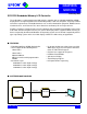
Epson Research and Development Vancouver Design Center Page 15 4 Functional Block Diagram 40k x 16-bit SRAM Memory Controller Register Power Save Clocks LCD Generic MPU MC68K SH-3 SH-4 LCD I/F Host I/F Look-Up Table Sequence Controller Bus Clock Memory Clock Pixel Clock Figure 4-1: System Block Diagram Showing Data Paths 4.1 Functional Block Descriptions 4.1.1 Host Interface The Host Interface provides the means for the CPU/MPU to communicate with the display buffer and internal registers.
Page 16 Epson Research and Development Vancouver Design Center 4.1.4 Look-Up Table The Look-Up Table contains three 256x4 Look-Up Tables or palettes, one for each primary color. In monochrome mode only the green Look-Up Table is used. 4.1.5 LCD Interface The LCD Interface performs frame rate modulation for passive LCD panels. It also generates the correct data format and timing control signals for various LCD and TFT/D-TFD panels. 4.1.6 Power Save Power Save contains the power save mode circuitry.
Epson Research and Development Vancouver Design Center Page 17 5 Pins 5.
Page 18 Epson Research and Development Vancouver Design Center 5.
Epson Research and Development Vancouver Design Center Pin Names Type Pin # Page 19 Cell RESET# State Description This pin has multiple functions. WE0# I 77 CS Input • For SH-3/SH-4 mode, this pin inputs the write enable signal for the lower data byte (WE0#). • For MC68K #1, this pin must be tied to IO VDD • For MC68K #2, this pin inputs the bus size bit 0 (SIZ0). • For Generic #1, this pin inputs the write enable signal for the lower data byte (WE0#).
Page 20 Pin Names Epson Research and Development Vancouver Design Center Type Pin # Cell RESET# State Description This pin has multiple functions. RD# I 76 CS • • • • For SH-3/SH-4 mode, this pin inputs the read signal (RD#). For MC68K #1, this pin must be tied to IO VDD. For MC68K #2, this pin inputs the bus size bit 1 (SIZ1). For Generic #1, this pin inputs the read command for the lower data byte (RD0#). • For Generic #2, this pin inputs the read command (RD#).
Epson Research and Development Vancouver Design Center Page 21 Pin Name Type Pin # Cell RESET# State Description FPLINE O 38 CN3 0 Line Pulse FPSHIFT O 28 CN3 0 Shift Clock LCDPWR O 43 CO1 0 Active high LCD Power Control This pin has multiple functions. DRDY O 42 CN3 • TFT/D-TFD Display Enable (DRDY). • LCD Backplane Bias (MOD). • Second Shift Clock (FPSHIFT2). 0 See Table 5-3: “LCD Interface Pin Mapping,” on page 23 for summary. 5.2.
Page 22 Epson Research and Development Vancouver Design Center 5.
Epson Research and Development Vancouver Design Center Page 23 5.
Page 24 Epson Research and Development Vancouver Design Center 6 D.C. Characteristics Table 6-1: Absolute Maximum Ratings Symbol Parameter Rating Units Core VDD Supply Voltage VSS - 0.3 to 4.0 V IO VDD Supply Voltage Core VDD to 7.0 V VIN Input Voltage VSS - 0.3 to IO VDD + 0.5 V VOUT Output Voltage VSS - 0.3 to IO VDD + 0.5 V TSTG Storage Temperature -65 to 150 °C TSOL Solder Temperature/Time 260 for 10 sec.
Epson Research and Development Vancouver Design Center Page 25 Table 6-4: Output Specifications Symbol Parameter Condition Min Typ Max Units IO VDD = 3.0V IOL (3.0V) Low Level Output Current VO = 0.4V, Type = 1 2 3 1.8 5 10 mA Type = 1 2 3 2 6 12 mA Type = 1 2 3 3 8 12 mA -1.8 -5 -10 mA -2 -6 -12 mA -3 -8 -12 mA IO VDD = 3.3V IOL (3.3V) Low Level Output Current VO = 0.4V, IO VDD = 5.0V IOL (5.0V) Low Level Output Current VO = 0.4V, IOH (3.
Page 26 Epson Research and Development Vancouver Design Center 7 A.C. Characteristics Conditions: IO VDD = 2.7 V to 5.0 V TA = -40° C to 85° C Trise and Tfall for all inputs must be < 5 nsec (10% ~ 90%) CL = 60pF (Bus/MPU Interface) CL = 60pF (LCD Panel Interface) 7.1 Bus Interface Timing 7.1.
Epson Research and Development Vancouver Design Center Page 27 Table 7-1: SH-4 Timing Symbol Parameter fCKIO Bus Clock frequency TCKIO Bus Clock period Min Max Units 50 MHz 1/fCKIO t2 Bus Clock pulse width low 8 ns t3 Bus Clock pulse width high 8 ns t4 A[16:0], RD/WR# setup to CKIO 0 ns t5 A[16:0], RD/WR# hold from CS# 0 ns t6 BS# setup 5 ns t7 BS# hold 5 ns t8 CSn# setup 0 ns t9 Falling edge RD# to DB[15:0] driven t10 CKIO to WE#, RD# high t11 Rising edge CSn#
Page 28 Epson Research and Development Vancouver Design Center 7.1.2 SH-3 Interface Timing TCKIO t2 t3 CKIO t5 t4 A[16:0], M/R# RD/WR# t6 t7 BS# t8 CSn# t9 t11 t10 WEn# RD# t13 t12 WAIT# Hi-Z Hi-Z t15 t14 D[15:0] (write) Hi-Z Hi-Z t17 t16 D[15:0] (read) Hi-Z VALID Hi-Z Figure 7-2: SH-3 Bus Timing Note The SH-3 Wait State Control Register for the area in which the S1D13705 resides must be set to a non-zero value.
Epson Research and Development Vancouver Design Center Page 29 Table 7-2: SH-3 Bus Timing Symbol Parameter fCKIO Bus Clock frequency TCKIO Bus Clock period Min Maxa Units 50 MHz 1/fCKIO t2 Bus Clock pulse width low 8 ns t3 Bus Clock pulse width high 8 ns t4 A[16:0], RD/WR# setup to CKIO 0 ns t5 A[16:0], RD/WR# hold from CS# 0 ns t6 BS# setup 5 ns t7 BS# hold 5 ns t8 CSn# setup 0 ns t9 Falling edge RD# to DB[15:0] driven t10 CKIO to WEn#, RD# high t11 25 ns 1.
Page 30 Epson Research and Development Vancouver Design Center 7.1.
Epson Research and Development Vancouver Design Center Page 31 7.1.
Page 32 Epson Research and Development Vancouver Design Center 7.1.
Epson Research and Development Vancouver Design Center Page 33 7.1.
Page 34 Epson Research and Development Vancouver Design Center 7.
Epson Research and Development Vancouver Design Center Page 35 Clock Input Waveform t PWH t PWL 90% V IH VIL 10% t tr f TBCLK Figure 7-8: Clock Input Requirements for BCLK Table 7-8: Clock Input Requirements for BCLK Symbol Parameter Min fBCLK Input Clock Frequency (BCLK) TBCLK Input Clock period (BCLK) tPWH Input Clock Pulse Width High (BCLK) 8 tPWL Input Clock Pulse Width Low (BCLK) 8 Max Units 50 MHz 1/fCLKI ns ns tf Input Clock Fall Time (10% - 90%) 5 ns tr Input Clock Ri
Page 36 Epson Research and Development Vancouver Design Center 7.3 Display Interface 7.3.
Epson Research and Development Vancouver Design Center Page 37 7.3.
Page 38 Epson Research and Development Vancouver Design Center 7.3.
Epson Research and Development Vancouver Design Center Page 39 t2 t1 Sync Timing Frame Pulse t3 t4 Line Pulse t5 DRDY (MOD) Data Timing Line Pulse t6 t8 t7 t9 t14 t11 t10 Shift Pulse t12 t13 1 FPDAT[7:4] 2 Note: For this timing diagram Mask FPSHIFT, REG[01h] bit 3, is set to 1 Figure 7-12: Single Monochrome 4-Bit Panel A.C. Timing Table 7-11: Single Monochrome 4-Bit Panel A.C. Timing Symbol t1 t2 t3 t4 t5 t6 t7 t8 t9 t10 t11 t12 t13 t14 1. 2. 3. 4. 5.
Page 40 Epson Research and Development Vancouver Design Center 7.3.
Epson Research and Development Vancouver Design Center Page 41 t1 t2 Sync Timing Frame Pulse t3 t4 Line Pulse t5 DRDY (MOD) Data Timing Line Pulse t6 t8 t7 t9 t14 t11 t10 Shift Pulse t12 t13 1 FPDAT[7:0] 2 Note: For this timing diagram Mask FPSHIFT, REG[01h] bit 3, is set to 1 Figure 7-14: Single Monochrome 8-Bit Panel A.C. Timing Table 7-12: Single Monochrome 8-Bit Panel A.C. Timing Symbol t1 t2 t3 t4 t5 t6 t7 t8 t9 t10 t11 t12 t13 t14 1. 2. 3. 4. 5.
Page 42 Epson Research and Development Vancouver Design Center 7.3.
Epson Research and Development Vancouver Design Center Page 43 t1 Sync Timing t2 Frame Pulse t3 t4 Line Pulse t5 DRDY (MOD) Data Timing Line Pulse t6 t8 t7 t9 t14 t11 t10 Shift Pulse t12 t13 1 FPDAT[7:4] 2 Figure 7-16: Single Color 4-Bit Panel A.C. Timing Table 7-13: Single Color 4-Bit Panel A.C. Timing Symbol t1 t2 t3 t4 t5 t6 t7 t8 t9 t10 t11 t12 t13 t14 1. 2. 3. 4. 5.
Page 44 Epson Research and Development Vancouver Design Center 7.3.
Epson Research and Development Vancouver Design Center Page 45 t1 Sync Timing t2 Frame Pulse t4 t3 Line Pulse Data Timing Line Pulse t6a t6b t8 t9 t14 t7a t11 t10 Shift Pulse 2 t7b Shift Pulse t12 t13 t12 t13 FPDAT[7:0] 1 2 Figure 7-18: Single Color 8-Bit Panel A.C. Timing (Format 1) Table 7-14: Single Color 8-Bit Panel A.C. Timing (Format 1) Symbol t1 t2 t3 t4 t6a t6b t7a t7b t8 t9 t10 t11 t12 t13 t14 1. 2. 3. 4. 5. 6. 7.
Page 46 Epson Research and Development Vancouver Design Center 7.3.
Epson Research and Development Vancouver Design Center Page 47 t1 Sync Timing t2 Frame Pulse t3 t4 Line Pulse t5 DRDY (MOD) Data Timing Line Pulse t6 t8 t7 t9 t14 t11 t10 Shift Pulse t12 t13 1 FPDAT[7:0] 2 Figure 7-20: Single Color 8-Bit Panel A.C. Timing (Format 2) Table 7-15: Single Color 8-Bit Panel A.C. Timing (Format 2) Symbol t1 t2 t3 t4 t5 t6 t7 t8 t9 t10 t11 t12 t13 t14 1. 2. 3. 4. 5.
Page 48 Epson Research and Development Vancouver Design Center 7.3.
Epson Research and Development Vancouver Design Center Page 49 t1 Sync Timing t2 Frame Pulse t4 t3 Line Pulse t5 DRDY (MOD) Data Timing Line Pulse t6 t8 t7 t9 t14 t11 t10 Shift Pulse t12 t13 1 2 FPDAT[7:0] Note: For this timing diagram Mask FPSHIFT, REG[01h] bit 3, is set to 1 Figure 7-22: Dual Monochrome 8-Bit Panel A.C. Timing Table 7-16: Dual Monochrome 8-Bit Panel A.C. Timing Symbol t1 t2 t3 t4 t5 t6 t7 t8 t9 t10 t11 t12 t13 t14 1. 2. 3. 5. 6.
Page 50 Epson Research and Development Vancouver Design Center 7.3.
Epson Research and Development Vancouver Design Center Page 51 t1 t2 Sync Timing Frame Pulse t4 t3 Line Pulse t5 DRDY (MOD) Data Timing Line Pulse t6 t8 t7 t9 t14 t11 t10 Shift Pulse t12 FPDAT[7:0] t13 1 2 Figure 7-24: Dual Color 8-Bit Panel A.C. Timing Table 7-17: Dual Color 8-Bit Panel A.C. Timing Symbol t1 t2 t3 t4 t5 t6 t7 t8 t9 t10 t11 t12 t13 t14 1. 2. 3. 5. 6.
Page 52 Epson Research and Development Vancouver Design Center 7.3.
Epson Research and Development Vancouver Design Center Page 53 t8 t9 Frame Pulse t12 Line Pulse t6 Line Pulse t7 t15 t17 DRDY t14 t1 t2 t11 t13 t3 t16 Shift Pulse t5 t4 1 FPDAT[11:0] 2 639 640 t10 Note: DRDY is used to indicate the first pixel Figure 7-26: TFT/D-TFD A.C.
Page 54 Epson Research and Development Vancouver Design Center Table 7-18: TFT/D-TFD A.C. Timing Symbol t1 t2 t3 t4 t5 t6 t7 t8 t9 t10 t11 t12 t13 t14 t15 t16 t17 1. 2. 3. 4. 5. 6. 7.
Epson Research and Development Vancouver Design Center Page 55 8 Registers 8.1 Register Mapping The S1D13705 registers are located in the upper 32 bytes of the 128K byte S1D13705 address range. The registers are accessible when CS# = 0 and AB[16:0] are in the range 1FFE0h through 1FFFFh. 8.2 Register Descriptions Unless specified otherwise, all register bits are reset to 0 during power up. All bits marked n/a should be programmed 0. REG[00h] Revision Code Register Address = 1FFE0h Read Only.
Page 56 Epson Research and Development Vancouver Design Center bit 4 FPLINE Polarity This bit controls the polarity of FPLINE in TFT/D-TFD mode (no effect in passive panel mode). When this bit = 0, FPLINE is active low. When this bit = 1, FPLINE is active high. bit 3 FPFRAME Polarity This bit controls the polarity of FPFRAME in TFT/D-TFD mode (no effect in passive panel mode). When this bit = 0, FPFRAME is active low. When this bit = 1, FPFRAME is active high.
Epson Research and Development Vancouver Design Center Page 57 REG[02h] Mode Register 1 Address = 1FFE2h Bit-Per-Pixel Bit 1 bits 7-6 Bit-Per-Pixel Bit 0 Read/Write. Input Clock divide (CLKI/2) High Performance Hardware Video Invert Enable Frame Repeat Display Blank Software Video Invert Bit-Per-Pixel Bits [1:0] These bits select the color or gray-scale depth (Display Mode).
Page 58 bit 4 Epson Research and Development Vancouver Design Center Input Clock Divide When this bit = 0, the Operating Clock(CLK) is the same as the Input Clock (CLKI). When this bit = 1, CLK = CLKI/2. In landscape mode PCLK=CLK and MCLK is selected as per Table 8-3: “High Performance Selection”. In SwivelView mode, MCLK and PCLK are derived from CLK as shown in Table 8-8: “Selection of PCLK and MCLK in SwivelView Mode,” on page 68. bit 3 Display Blank This bit blanks the display image.
Epson Research and Development Vancouver Design Center Page 59 REG[03h] Mode Register 2 Address = 1FFE3h n/a Read/Write n/a n/a n/a LCDPWR Override Hardware Power Save Enable Software Power Save Bit 1 Software Power Save Bit 0 bit 3 LCDPWR Override This bit is used to override the panel on/off sequencing logic. When this bit = 0, LCDPWR and the panel interface signals are controlled by the sequencing logic.
Page 60 Epson Research and Development Vancouver Design Center REG[04h] Horizontal Panel Size Register Address = 1FFE4h n/a Read/Write Horizontal Horizontal Horizontal Horizontal Horizontal Horizontal Horizontal Panel Size Bit Panel Size Bit Panel Size Bit Panel Size Bit Panel Size Bit Panel Size Bit Panel Size Bit 6 5 4 3 2 1 0 bits 6-0 Horizontal Panel Size Bits [6:0] This register determines the horizontal resolution of the panel.
Epson Research and Development Vancouver Design Center Page 61 REG[07h] FPLINE Start Position Address = 1FFE7h n/a n/a bits 4-0 Read/Write FPLINE Start Position Bit 4 n/a FPLINE Start Position Bit 3 FPLINE Start Position Bit 2 FPLINE Start Position Bit 1 FPLINE Start Position Bit 0 FPLINE Start Position These bits are used in TFT/D-TFD mode to specify the position of the FPLINE pulse.
Page 62 Epson Research and Development Vancouver Design Center REG[0Ah] Vertical Non-Display Period Address = 1FFEAh Vertical NonDisplay Status Vertical NonDisplay Period Bit 5 n/a Read/Write Vertical NonDisplay Period Bit 4 Vertical NonDisplay Period Bit 3 Vertical NonDisplay Period Bit 2 Vertical NonDisplay Period Bit 1 Vertical NonDisplay Period Bit 0 bit 7 Vertical Non-Display Status This bit =1 during the Vertical Non-Display period.
Epson Research and Development Vancouver Design Center Page 63 REG[0Ch] Screen 1 Start Address Register (LSB) Address = 1FFECh Read/Write Screen 1 Start Screen 1 Start Screen 1 Start Screen 1 Start Screen 1 Start Screen 1 Start Screen 1 Start Screen 1 Start Address Address Address Address Address Address Address Address Bit 7 Bit 6 Bit 5 Bit 4 Bit 3 Bit 2 Bit 1 Bit 0 REG[0Dh] Screen 1 Start Address Register (MSB) Address = 1FFEDh Read/Write Screen 1 Start Screen 1 Start Screen 1 Start Screen 1 Start
Page 64 Epson Research and Development Vancouver Design Center REG[11h] Memory Address Offset Register Address = 1FFF1h Memory Address Offset Bit 7 Memory Address Offset Bit 6 bits 7-0 Memory Address Offset Bit 5 Read/Write Memory Address Offset Bit 4 Memory Address Offset Bit 3 Memory Address Offset Bit 2 Memory Address Offset Bit 1 Memory Address Offset Bit 0 Memory Address Offset Bits [7:0] (Landscape Modes Only) This register is used to create a virtual image by setting a word offset between
Epson Research and Development Vancouver Design Center Page 65 (REG[0Dh], REG[0Ch]) Words Line 0 Last Pixel Address + REG[11h] Words Line 0 Last Pixel Address=((REG[0Dh], REG[0Ch]) + (8(REG[04h]+1) × BPP/16)) Words Line 0 Line 1 Image 1 ((REG[06h], REG[05])+1) Lines Line=(REG[13h], REG[12h]) Image 2 (REG[0Fh], REG[0Eh]) Words REG[11h] Words 8(REG[04h]+1) Pixels Where: (REG[0Dh], REG[0Ch]) is the Screen 1 Start Word Address BPP is Bits-per-Pixel as set by REG[02h] bits 7:6 REG[11h] is the Address Pi
Page 66 Epson Research and Development Vancouver Design Center REG[17h] Look-Up Table Data Register Address = 1FFF7h LUT Data Bit 3 LUT Data Bit 2 bits 7-4 LUT Data Bit 1 Read/Write LUT Data Bit 0 n/a n/a n/a n/a LUT Data Bits [3:0] This register is used to read/write the RGB Look-Up Tables. This register accesses the entry at the pointer controlled by the Look-Up Table Address Register (REG[15h]). Accesses to the Look-Up Table Data Register automatically increment the pointer.
Epson Research and Development Vancouver Design Center Page 67 REG[19h] GPIO Status/Control Register Address = 1FFF9h n/a bits 4-0 n/a Read/Write GPIO4 Pin IO GPIO3 Pin IO Status Status n/a GPIO2 Pin IO Status GPIO1 Pin IO GPIO0 Pin IO Status Status GPIO[4:0] Status When the GPIOn pin is configured as an input, the corresponding GPIO Status bit is used to read the pin input. See REG[18h] above.
Page 68 Epson Research and Development Vancouver Design Center bit 2 reserved reserved bits must be set to 0. bits 1-0 SwivelView Mode Pixel Clock Select Bits [1:0] These two bits select the Pixel Clock (PCLK) source in SwivelView Mode - these bits have no effect in Landscape Mode. The following table shows the selection of PCLK and MCLK in SwivelView Mode - see Section 12, “SwivelView™” on page 77 for details.
Epson Research and Development Vancouver Design Center Page 69 9 Frame Rate Calculation The following formulae are used to calculate the display frame rate.
Page 70 Epson Research and Development Vancouver Design Center 10 Display Data Formats 1-bpp: Byte 0 bit 7 A0 bit 0 A1 A2 A3 A4 A5 A6 P0 P1 P2 P3 P4 P5 P6 P7 A7 Pn = (An) Panel Display Host Address 2-bpp: Display Memory bit 7 bit 0 Byte 0 A0 B0 A1 B1 A2 B2 A3 B3 Byte 1 A4 B4 A5 B5 A6 B6 A7 B7 P0 P1 P2 P3 P4 P5 P6 P7 Pn = (An, Bn) Panel Display Host Address Display Memory 4-bpp: bit 7 bit 0 Byte 0 A0 B0 C0 D0 A1 B1 C1 D1 Byte 1 A2 B2 C2 D2 A3 B3 C3 D3
Epson Research and Development Vancouver Design Center Page 71 11 Look-Up Table Architecture The following figures are intended to show the display data output path only. Note When Video Data Invert is enabled the video data is inverted after the Look-Up Table. 11.1 Monochrome Modes The green Look-Up Table (LUT) is used for all monochrome modes.
Page 72 Epson Research and Development Vancouver Design Center 4 Bit-per-pixel Monochrome Mode Green Look-Up Table 256x4 00 01 02 03 04 05 06 07 08 09 0A 0B 0C 0D 0E 0F 10 0000 0001 0010 0011 0100 0101 0110 0111 1000 1001 1010 1011 1100 1101 1110 1111 4-bit Gray Data FC FD FE FF 4 bit-per-pixel data from Display Buffer = unused Look-Up Table entries Figure 11-3: 4 Bit-per-pixel Monochrome Mode Data Output Path S1D13705 X27A-A-001-10 Hardware Functional Specification Issue Date: 02/02/01
Epson Research and Development Vancouver Design Center Page 73 11.
Page 74 Epson Research and Development Vancouver Design Center 2 Bit-per-pixel Color Mode Red Look-Up Table 256x4 00 01 02 03 04 00 01 10 11 4-bit Red Data 00 01 10 11 4-bit Green Data 00 01 10 11 4-bit Blue Data FC FD FE FF Green Look-Up Table 256x4 00 01 02 03 04 FC FD FE FF Blue Look-Up Table 256x4 00 01 02 03 04 FC FD FE FF 2 bit-per-pixel data from Display Buffer = unused Look-Up Table entries Figure 11-5: 2 Bit-per-pixel Color Mode Data Output Path S1D13705 X27A-A-001-10 Hardware Function
Epson Research and Development Vancouver Design Center Page 75 4 Bit-per-pixel Color Mode Red Look-Up Table 256x4 00 01 02 03 04 05 06 07 08 09 0A 0B 0C 0D 0E 0F 10 0000 0001 0010 0011 0100 0101 0110 0111 1000 1001 1010 1011 1100 1101 1110 1111 4-bit Red Data FC FD FE FF Green Look-Up Table 256x4 00 01 02 03 04 05 06 07 08 09 0A 0B 0C 0D 0E 0F 10 0000 0001 0010 0011 0100 0101 0110 0111 1000 1001 1010 1011 1100 1101 1110 1111 4-bit Green Data FC FD FE FF Blue Look-Up Table 256x4 00 01 02 03 04 05 06
Page 76 Epson Research and Development Vancouver Design Center 8 Bit-per-pixel Color Mode Red Look-Up Table 256x4 00 01 02 03 04 05 06 07 0000 0000 0000 0001 0000 0010 0000 0011 0000 0100 0000 0101 0000 0110 0000 0111 F8 F9 FA FB FC FD FE FF 1111 1000 1111 1001 1111 1010 1111 1011 1111 1100 1111 1101 1111 1110 1111 1111 4-bit Red Data Green Look-Up Table 256x4 00 01 02 03 04 05 06 07 0000 0000 0000 0001 0000 0010 0000 0011 0000 0100 0000 0101 0000 0110 0000 0111 F8 F9 FA FB FC FD FE FF 1111 1000 1
Epson Research and Development Vancouver Design Center Page 77 12 SwivelView™ Many of todays applications use the LCD panel in a portrait orientation. In this case it becomes necessary to “rotate” the displayed image by 90°. This rotation can be done by software at the expense of performance or, it can be done by the S1D13705 hardware with no CPU penalty. There are two SwivelView modes: Default SwivelView Mode and Alternate SwivelView Mode. 12.
Page 78 Epson Research and Development Vancouver Design Center 12.1.1 How to Set Up Default SwivelView Mode The following describes the register settings needed to set up Default SwivelView Mode for a 240x320x8 bpp image: • Select Default SwivelView Mode: REG[1Bh] bit 7 = 1 and bit 6 = 0 • The display refresh circuitry starts at pixel “B”, therefore the Screen 1 Start Address register must be programmed with the address of pixel “B”, i.e.
Epson Research and Development Vancouver Design Center Page 79 12.2 Alternate SwivelView Mode Alternate SwivelView Mode may be used when the virtual image size of Default SwivelView Mode cannot be contained in the 80K byte integrated frame buffer. For example, the panel size is 480x320 and the display mode is 4 bit-per-pixel. The minimum virtual image size for Default SwivelView Mode would be 480x512 which requires 122,880 bytes.
Page 80 Epson Research and Development Vancouver Design Center 12.2.1 How to Set Up Alternate SwivelView Mode The following describes the register settings needed to set up Alternate SwivelView Mode for a 320x480x4 bpp image.
Epson Research and Development Vancouver Design Center Page 81 12.3 Comparison Between Default and Alternate SwivelView Modes Table 12-1: Default and Alternate SwivelView Mode Comparison Item Default SwivelView Mode Alternate SwivelView Mode The width of the rotated image must be a power of 2. In most cases, a virtual image is required where the right-hand side of the virtual image is unused and memory is wasted.
Page 82 Epson Research and Development Vancouver Design Center 13 Power Save Modes Two Power Save Modes have been incorporated into the S1D13705 to accommodate the need for power reduction in the hand-held devices market.
Epson Research and Development Vancouver Design Center Page 83 13.
Page 84 Epson Research and Development Vancouver Design Center RESET# Software Power Save REG[03h] bits [1:0] 00 11 00 11 or Hardware Power Save LCDPWR Power Save Mode Panel Interface Output Signals (except LCDPWR) 0 frame power-up 127 frames power-down 0 frame power-up Figure 13-1: Panel On/Off Sequence After chip reset, LCDPWR is inactive and the rest of the panel interface output signals are held “low”. Software initializes the chip (i.e.
Epson Research and Development Vancouver Design Center Page 85 13.6 Clock Requirements The following table shows what clock is required for which function in the S1D13705 Table 13-5: S1D13705 Internal Clock Requirements Function BCLK CLKI Register Read/Write Is required during register accesses. BCLK can be shut down between accesses: allow eight BCLK pulses plus 12 MCLK pulses (8TBCLK + 12TMCLK) after the last access before shutting BCLK off.
Page 86 Epson Research and Development Vancouver Design Center 14 Mechanical Data QFP14 - 80 pin Unit: mm 14.0 ± 0.4 12.0 ± 0.1 60 41 61 14.0 ± 0.4 12.0 ± 0.1 40 Index 80 21 0.125 1.4 ± 0.1 + 0.05 - 0.025 1 0.5 + 0.1 20 0.18 - 0.05 0.1 0~10° 0.5 ± 0.2 1.
Epson Research and Development Vancouver Design Center Page 87 15 Sales and Technical Support Japan Seiko Epson Corporation Electronic Devices Marketing Division 421-8, Hino, Hino-shi Tokyo 191-8501, Japan Tel: 042-587-5812 Fax: 042-587-5564 http://www.epson.co.jp North America Epson Electronics America, Inc. 150 River Oaks Parkway San Jose, CA 95134, USA Tel: (408) 922-0200 Fax: (408) 922-0238 http://www.eea.epson.com Taiwan Epson Taiwan Technology & Trading Ltd. 10F, No. 287 Nanking East Road Sec.
Page 88 Epson Research and Development Vancouver Design Center THIS PAGE LEFT BLANK S1D13705 X27A-A-001-10 Hardware Functional Specification Issue Date: 02/02/01
S1D13705 Embedded Memory LCD Controller Programming Notes and Examples Document Number: X27A-G-002-03 Copyright © 2001, 2002 Epson Research and Development, Inc. All Rights Reserved. Information in this document is subject to change without notice. You may download and use this document, but only for your own use in evaluating Seiko Epson/EPSON products. You may not modify the document. Epson Research and Development, Inc.
Page 2 Epson Research and Development Vancouver Design Center THIS PAGE LEFT BLANK S1D13705 X27A-G-002-03 Programming Notes and Examples Issue Date: 02/01/22
Epson Research and Development Vancouver Design Center Page 3 Table of Contents 1 Introduction . . . . . . . . . . . . . . . . . . . . . . . . . . . . . . . . . . . . . . . . 7 2 Initialization . . . . . . . . 2.1 Display Buffer Location 2.2 Register Values . . . . 2.3 Frame Rate Calculation . 3 Memory Models . . . . . . . . . . . . . . . . 3.1 1 Bit-Per-Pixel (2 Colors/Gray Shades) . . 3.2 2 Bit-Per-Pixel (4 Colors/Gray Shades) . . 3.3 4 Bit-Per-Pixel (16 Colors/Gray Shades) . . 3.
Page 4 Epson Research and Development Vancouver Design Center 8 Identifying the S1D13705 . . . . . . . . . . . . . . . . . . . . . . . . . . . . . . . .47 9 Hardware Abstraction Layer (HAL) . . . . . . . . . . . . . 9.1 Introduction . . . . . . . . . . . . . . . . . . . . 9.2 Contents of the HAL_STRUCT . . . . . . . . . . . . 9.3 Using the HAL library . . . . . . . . . . . . . . . . 9.4 API for 13705HAL . . . . . . . . . . . . . . . . . 9.4.1 Initialization . . . . . . . . . . . . . . . . . . . . . .
Epson Research and Development Vancouver Design Center Page 5 List of Tables Table 2-1: Table 4-1: Table 4-2: Table 4-3: Table 4-4: Table 4-5: Table 4-6: Table 4-7: Table 5-1: Table 7-1: Table 9-1: S1D13705 Initialization Sequence . . . . . . . . . . . . . . . . . Recommended LUT Values for 1 Bpp Color Mode . . . . . . . . . Example LUT Values for 2 Bpp Color Mode . . . . . . . . . . . .
Page 6 Epson Research and Development Vancouver Design Center THIS PAGE LEFT BLANK S1D13705 X27A-G-002-03 Programming Notes and Examples Issue Date: 02/01/22
Epson Research and Development Vancouver Design Center Page 7 1 Introduction This guide demonstrates how to program the S1D13705 Embedded Memory Color LCD Controller. The guide presents the basic concepts of the LCD controller and provides methods to directly program the registers. It explains some of the advanced techniques used and the special features of the S1D13705. The guide also introduces the Hardware Abstraction Layer (HAL), which is designed to make programming the S1D13705 as easy as possible.
Page 8 Epson Research and Development Vancouver Design Center 2 Initialization Prior to doing anything else with the S1D13705 the controller must be initialized. Initialization is the process of setting up the control registers to a known state in order to generate proper display signals. 2.1 Display Buffer Location Before we can perform the initialization we have to know where to find the S1D13705 display memory and control registers. The S1D13705 contains 80 kilobytes of internal display memory.
Epson Research and Development Vancouver Design Center Page 9 Table 2-1: S1D13705 Initialization Sequence Register Value (hex) [01] 0010 0011 (23) Select a passive, Single, Color panel with an 8-bit data width Notes [02] 1100 0000 (C0) Select 8-bit per pixel color depth [03] 0000 0011 (03) Select normal power operation [04] 0010 0111 (27) Horizontal display size = (Reg[04]+1)*8 = (39+1) * 8 = 320 pixels [05] 1110 1111 (EF) [06] 0000 0000 (00) Vertical display size = Reg[06][05] + 1 = 00
Page 10 Epson Research and Development Vancouver Design Center The following are the formulae for determining the frame rate of a panel.
Epson Research and Development Vancouver Design Center Page 11 This routine first performs a formula rearrangement so that HNDP or VNDP can be solved. Start with VNDP set to a small value. Loop increasing VNDP and solving the equation for HNDP until satisfactory HNDP and VNDP values are found. If no satisfactory values are found then divide CLKI and repeat the process. If a satisfactory frame rate still can’t be reached - return an error.
Page 12 Epson Research and Development Vancouver Design Center 3 Memory Models The S1D13705 is capable of operating at four different color depths. For each color depth the data format is packed pixel. S1D13705 packed pixel modes can range from one byte containing eight adjacent pixels (1-bpp) to one byte containing just one pixel (8-bpp). Packed pixel data may be envisioned as a stream of pixels. In this stream, pixels are packed in adjacent to each other.
Epson Research and Development Vancouver Design Center Page 13 3.2 2 Bit-Per-Pixel (4 Colors/Gray Shades) 2-bit pixels support four color/gray shades. In this memory format each byte of display buffer contains four adjacent pixels. Setting or resetting any pixel requires reading the entire byte, masking out the appropriate bits and, if necessary, setting bits to “1”. Color panels derive their four colors by indexing into positions 0 through 3 of the Look-Up Table.
Page 14 Epson Research and Development Vancouver Design Center 3.4 Eight Bit-Per-Pixel (256 Colors) In eight bit-per-pixel mode one byte of display buffer represents one pixel on the display. At this color depth the read-modify-write cycles, required by the lessor pixel depths, are eliminated. When using a color panel, each byte of display memory acts as and index to one element of the LUT. The displayed color is arrived at by taking the display memory value as an index into the LUT.
Epson Research and Development Vancouver Design Center Page 15 4 Look-Up Table (LUT) This section is supplemental to the description of the Look-Up Table architecture found in the S1D13705 Hardware Functional Specification. Covered here is a review of the LUT registers, recommendations for the color and gray shade LUT values, and additional programming considerations for the LUT. Refer to the S1D13705 Hardware Functional Specification, document number X27A-A-001-xx for more detail.
Page 16 Epson Research and Development Vancouver Design Center 4.1 Look-Up Table Registers REG[15h] Look-Up Table Address Register LUT Address Bit 7 LUT Address Bit 6 LUT Address Bit 5 LUT Address Bit 4 Read/Write LUT Address Bit 3 LUT Address Bit 2 LUT Address Bit 1 LUT Address Bit 0 LUT Address The LUT address register selects which of the 256 LUT entries will be accessed.
Epson Research and Development Vancouver Design Center Page 17 4.2 Look-Up Table Organization 4.2.1 Color Modes 1 bpp color When the S1D13705 is configured for 1 bpp color mode, the LUT is limited to selecting colors from the first two entries. The two LUT entries can be any two RGB values but are typically set to black-and-white. Each byte in the display buffer contains eight adjacent pixels. If a bit has a value of “0” then the color in LUT 0 index is displayed.
Page 18 Epson Research and Development Vancouver Design Center 2 bpp color When the S1D13705 is configured for 2 bpp color mode, the displayed colors are selected from the first four entries of the Look-Up Table. The LUT entries may be set to any of the 4096 possible colors. Each byte in the display buffer contains four adjacent pixels. If a bit combination has a value of “00” then the color in LUT index 0 is displayed. A bit value of “01” results in the color in LUT index 1 being displayed.
Epson Research and Development Vancouver Design Center Page 19 4 bpp color When the S1D13705 is configured for 4 bpp color mode, the displayed colors are selected from the first sixteen entries of the Look-Up Table. The LUT entries may be set to any of the 4096 possible colors. Each byte in the display buffer contains two adjacent pixels. If a nibble has a value of “0000” then the color in LUT index 0 is displayed. A nibble value of “0001” results in the color in LUT index 1 being displayed.
Page 20 Epson Research and Development Vancouver Design Center 8 bpp color When the S1D13705 is configured for 8 bpp color mode the entire Look-Up Table is used to display images. Each of the LUT entries may be set to any of the 4096 possible colors. Each byte in the display buffer represents one pixels. The byte value is used directly as an index into one of the 256 LUT entries.
Epson Research and Development Vancouver Design Center Page 21 Table 4-4: Suggested LUT Values to Simulate VGA Default 256 Color Palette (Continued) Index R G B Index R G B Index R G B Index R G B 1C B0 B0 B0 5C F0 F0 B0 9C 70 50 70 DC 20 40 40 1D C0 C0 C0 5D E0 F0 B0 9D 70 50 60 DD 20 30 40 1E E0 E0 E0 5E D0 F0 B0 9E 70 50 60 DE 20 30 40 1F F0 F0 F0 5F C0 F0 B0 9F 70 50 50 DF 20 20 40 20 00 00 F0 60 B0 F0 B0 A0 70 5
Page 22 Epson Research and Development Vancouver Design Center 4.2.2 Gray Shade Modes Gray shade modes are monochrome display modes. Monochrome display modes use the Look-Up Table in a very similar fashion to the color modes. This most significant difference is that the monochrome display modes use only the intensity of the green element of the Look-Up Table to form the gray level.
Epson Research and Development Vancouver Design Center Page 23 The following table shows the example values for 2 bit-per-pixel display mode. Table 4-6: Suggested Values for 2 Bpp Gray Shade Index Red Green Blue 0 00 00 00 1 00 50 00 2 00 A0 00 3 00 F0 00 4 00 00 00 ...
Page 24 Epson Research and Development Vancouver Design Center 4 bpp gray shade When the S1D13705 is configured for 4 bpp gray shade mode the displayed colors are selected from the green values of the first sixteen entries of the Look-Up Table. Each of the sixteen entries can be set to any of the sixteen possible intensity levels. Each byte in the display buffer contains two adjacent pixels. If a nibble pattern is “0000” then the green intensity of LUT index 0 is displayed.
Epson Research and Development Vancouver Design Center Page 25 5 Advanced Techniques This section contains programming suggestions for the following: • virtual display • panning and scrolling • split screen display 5.1 Virtual Display Virtual display refers to the situation where the image to be viewed is larger than the physical display. The difference can be in the horizontal, vertical or both dimensions. To view the image, the display is used as a window into the display buffer.
Page 26 Epson Research and Development Vancouver Design Center 5.1.1 Registers REG[11h] Memory Address Offset Register Memory Address Offset Bit 7 Memory Address Offset Bit 6 Memory Address Offset Bit 5 Memory Address Offset Bit 4 Memory Address Offset Bit 3 Memory Address Offset Bit 2 Memory Address Offset Bit 1 Memory Address Offset Bit 0 Memory Address Offset Register REG[11h] forms an 8-bit value called the Memory Address Offset.
Epson Research and Development Vancouver Design Center Page 27 Example 2: From the above, what is the maximum number of lines our image can contain? Step 1: Calculate the number of bytes on each line. bytes_per_line = pixels_per_line / pixels_per_byte = 640 / 4 = 160 Each line of the display requires 160 bytes. Step 2: Calculate the number of lines the S1D13705 is capable of. total_lines = memory / bytes_per_line = 81920 / 160 = 512 We can display a maximum of 512 lines.
Page 28 Epson Research and Development Vancouver Design Center 5.2.
Epson Research and Development Vancouver Design Center Page 29 5.2.2 Examples For the following examples we base our calculations on a 4 bit-per-pixel image displayed on a 256w x 64h panel. We have set up a virtual size of 320w x 240h. Width is greater than height so we are in landscape display mode. Refer to Section 2, “Initialization” on page 8 and Section 5.1, “Virtual Display” on page 25 for assistance with these settings. These examples are shown using a C-like syntax.
Page 30 Epson Research and Development Vancouver Design Center Example 4: Scrolling (Up and Down) To scroll down, increase the value in the Screen 1 Display Start Address Register by the number of words in one virtual scan line. To scroll up, decrease the value in the Screen 1 Display Start Address Register by the number of words in one virtual scan line.
Epson Research and Development Vancouver Design Center Page 31 5.3 Split Screen Occasionally the need arises to display two different but related images. Take, for example, a game where the main play area requires rapid updates and game status, displayed at the bottom of the screen, requires infrequent updates. The Split Screen feature of the S1D13705 allows a programmer to setup a display in such a manor. When correctly configured the programmer has only to update the main area on a regular basis.
Page 32 Epson Research and Development Vancouver Design Center 5.3.1 Registers Split screen operation is performed primarily by manipulating three register sets. Screen 1 Start Address and Screen 2 Start Address determine from where in display memory the first and second images will be taken from. The Vertical Size registers determine how many lines Screen 1 will use. The following is a description of the registers used to do split screen.
Epson Research and Development Vancouver Design Center Page 33 REG[0Eh] Screen 2 Display Start Address 0 (LSB) Start Addr Bit 7 Start Addr Bit 6 Start Addr Bit 5 Start Addr Bit 4 Start Addr Bit 3 Start Addr Bit 2 Start Addr Bit 1 Start Addr Bit 0 Start Addr Bit 11 Start Addr Bit 10 Start Addr Bit 9 Start Addr Bit 8 REG[0Fh] Screen 2 Display Start Address 1 (MSB) Start Addr Bit 15 Start Addr Bit 14 Start Addr Bit 13 Start Addr Bit 12 Screen 2 Start Address Registers These three registers f
Page 34 Epson Research and Development Vancouver Design Center 5.3.2 Examples Example 5: Display 200 scanlines of image 1 and 40 scanlines of image 2. Image 2 is located first (offset 0) in the display buffer followed immediately by image 1. Assume a 320x240 display and a color depth of 4 bpp. 1. Calculate the Screen 1Vertical Size register values. vertical_size = 200 = C8h Write the Vertical Size LSB, REG[12h], with C8h and Vertical Size MSB, REG[13h], with a 00h. 2.
Epson Research and Development Vancouver Design Center Page 35 6 LCD Power Sequencing and Power Save Modes 6.1 LCD Power Sequencing Correct power sequencing is required to prevent long term damage to LCD panels and to avoid unsightly “lines” during power-up and power-down. Power Sequencing allows the LCD power supply to discharge prior to shutting down the LCD logic signals.
Page 36 Epson Research and Development Vancouver Design Center 6.3 LCD Enable/Disable The descriptions below cover manually powering the LCD panel up and down. Use the sequences described in this section if the power supply connected to the panel requires more than 127 frames to discharge on power-down, or if the panel requires starting the LCD logic well in advance of enabling LCD power. Currently there are no known circumstances where the LCD logic must be active well in advance of LCD power.
Epson Research and Development Vancouver Design Center Page 37 7 Hardware Rotation 7.1 Introduction To Hardware Rotation Many of todays applications use the LCD panel in a portrait orientation (typically LCD panels are landscape oriented). In this case it becomes necessary to “rotate” the displayed image. This rotation can be done by software at the expense of performance or, as with the S1D13705, it can be done by hardware with no performance penalty.
Page 38 Epson Research and Development Vancouver Design Center physical memory start address 256 E 240 C A display start address 256 D portrait window portrait window 320 E B B A D C 320 240 image seen by programmer = image in display buffer image refreshed by S1D13705 Figure 7-1: Relationship Between the Default Mode Screen Image and the Image Refreshed by S1D13705 From the programmers perspective the memory is laid out as shown on the left.
Epson Research and Development Vancouver Design Center Page 39 7.3 Alternate Portrait Mode Alternate portrait mode does not impose the power of two line width. To rotated the image on 240 line panel requires a portrait stride of 240 pixels. Alternate portrait mode is capable of scrolling by one line at a time in response to changes to the Start Address Registers. However, to achieve the same frame rate requires a 2 x faster input clock, therefore using more power.
Page 40 Epson Research and Development Vancouver Design Center 7.4 Registers This section describes the registers used to set portrait mode operation.
Epson Research and Development Vancouver Design Center Page 41 The portrait mode select bit selects between the “Default Mode” and the “Alternate Mode”. Setting this bit to “0” selects the default portrait mode while setting this bit to “1” enables the alternate portrait mode. Portrait Mode Memory Clock Select is another power saving measure which can be enabled if the final MCLK value is less than or equal to 25 MHz.
Page 42 Epson Research and Development Vancouver Design Center 7.5 Limitations The only limitation to using portrait mode on the S1D13705 is that split screen operation is not supported. A comparison of the two portrait modes is as follows: Table 7-1: Default and Alternate Portrait Mode Comparison Item Default Portrait Mode Alternate Portrait Mode The width of the rotated image must be a power of 2.
Epson Research and Development Vancouver Design Center Page 43 7.6 Examples Example 6: Enable default portrait mode for a 320x240 panel at 4 bpp. Before switching to portrait mode from landscape mode, display memory should be cleared to make the user perceived transition smoother. Images in display memory are not rotated automatically by hardware and a garbled image would be visible for a short period of time if video memory is not cleared.
Page 44 Epson Research and Development Vancouver Design Center Example 7: Enable alternate portrait mode for a 320x240 panel at 4 bpp. Note As we have to perform a frame rate calculation for this mode we need to know the following panel characteristics: 320x240 8-bit color to be run at 80 Hz with a 16 MHz input clock. As in the previous example, before switching to portrait mode, display memory should be cleared.
Epson Research and Development Vancouver Design Center Page 45 PCLK FrameRate = ----------------------------------------------------------------------------------------( HDP + HNDP ) × ( VDP + VNDP ) 16, 000, 000 -----------------------------2 FrameRate = ------------------------------------------------------- = 80.69 ( 320 + 88 ) × ( 240 + 3 ) For this example the Horizontal Non-Display register [REG[08h]) needs to be set to 07h and the Vertical Non-Display register (REG[0Ah]) needs to be set to 03h.
Page 46 Epson Research and Development Vancouver Design Center Example 8: Pan the above portrait mode image to the right by 4 pixels then scroll it up by 6 pixels. To pan by four pixels the start address needs to be advanced. 1. Calculate the number of bytes to change start address by. Bytes = Pixels x BitsPerPixel / 8 = 4 x 4 / 8 = 2 bytes 2. Increment the start address registers by the just calculated value.
Epson Research and Development Vancouver Design Center Page 47 8 Identifying the S1D13705 There are several similar products in the 135X and 137X LCD controller families. Products which can share significant portions of a generic code base. It may be important for a program to identify between products at run time. Identification of the S1D13705 can be performed any time after the system has been powered up by reading REG[00h], the Revision Code register.
Page 48 Epson Research and Development Vancouver Design Center 9 Hardware Abstraction Layer (HAL) 9.1 Introduction The HAL is a processor independent programming library provided by Epson. The HAL was developed to aid the implementation of internal test programs, and provides an easy, consistent method of programming the S1D13705 on different processor platforms. The HAL also allows for easier porting of programs between S1D1370X products.
Epson Research and Development Vancouver Design Center Page 49 9.3 Using the HAL library To utilize the HAL library, the programmer must include two “.h” files in their code. “Hal.h” contains the HAL library function prototypes and structure definitions, and “appcfg.h” contains the instance of the HAL_STRUCT that is defined in “Hal.h” and configured by 13705CFG.EXE. For a more thorough example of using the HAL see Section 10.1, “Sample code using the S1D13705 HAL API” on page 66.
Page 50 Epson Research and Development Vancouver Design Center Table 9-1: HAL Functions (Continued) Function Description Register / Memory Access: seSetReg Write a Byte value to the specified S1D13705 register seGetReg Read a Byte value from the specified S1D13705 register seWriteDisplayBytes Write one or more bytes to the display buffer at the specified offset seWriteDisplayWords Write one or more words to the display buffer at the specified offset seWriteDisplayDwords Write one or more dwords
Epson Research and Development Vancouver Design Center Page 51 9.4.1 Initialization The following section describes the HAL functions dealing with S1D13705 initialization. Typically a programmer has only to concern themselves with calls to seRegisterDevice() and seSetInit(). int seRegisterDevice(const LPHAL_STRUC lpHalInfo) Description: This function registers the S1D13705 device parameters with the HAL library. The device parameters include address range, register values, desired frame rate, etc.
Page 52 Epson Research and Development Vancouver Design Center 9.4.2 General HAL Support Functions in this group do not fit into any specific category of support. They provide a miscellaneous range of support for working with the S1D13705 int seGetId(int * pId) Description: Reads the S1D13705 revision code register to determine the chip product and revisions. The interpreted value is returned in pID. Parameters: pId - pointer to an integer which will receive the controller ID.
Epson Research and Development Vancouver Design Center Page 53 int seSetBitsPerPixel(int BitsPerPixel) Description: This routine sets the display color depth. After performing validity checks to ensure the requested video mode can be set the appropriate registers are changed and the Look-Up Table is set its default values appropriate to the color depth. This call is similar to a mode set call on a standard VGA. Parameter: BitsPerPixel - desired color depth in bits per pixel.
Page 54 Epson Research and Development Vancouver Design Center int seGetScreenSize(int * Width, int * Height) Description: Retrieves the width and height in pixels of the display surface. The width and height are derived by reading the horizontal and vertical size registers and calculating the dimensions. Virtual dimensions are not taken into account for this calculation. When the display is in portrait mode the dimensions will be swapped. (i.e.
Epson Research and Development Vancouver Design Center Page 55 int seSetHighPerformance(BOOL OnOff) Description: This function call enables or disable the high performance bit of the S1D13705. When high performance is enabled then MClk equals PClk for all video display resolutions. In the high performance state CPU to video memory performance is improved at the cost of higher power consumption. When high performance is disabled then MClk ranges from PClk/1 at 8 bit-per-pixel to PClk/8 at 1 bit-per-pixel.
Page 56 Epson Research and Development Vancouver Design Center int seSplitInit(WORD Scrn1Addr, WORD Scrn2Addr) Description: This function prepares the system for split screen operation. In order for split screen to function the starting address in the display buffer for the upper portion(screen 1) and the lower portion (screen 2) must be specified. Screen 1 is always displayed above screen 2 on the display regardless of the location of their start addresses.
Epson Research and Development Vancouver Design Center Page 57 int seVirtInit(DWORD VirtX, DWORD * VirtY) Description: This function prepares the system for virtual screen operation. The programmer passes the desired virtual width in pixels. When the routine returns VirtY will contain the maximum number of line that can be displayed at the requested virtual width. Parameter: VirtX VirtY - horizontal size of virtual display in pixels.
Page 58 Epson Research and Development Vancouver Design Center 9.4.4 Register / Memory Access The Register/Memory Access functions provide access to the S1D13705 registers and display buffer through the HAL. int seGetReg(int Index, BYTE * pValue) Description: Reads the value in the register specified by index. Parameters: Index pValue Return Value: ERR_OK - register index to read - pointer to a BYTE to receive the register value.
Epson Research and Development Vancouver Design Center Page 59 int seReadDisplayDword(DWORD Offset, DWORD *pDword) Description: Reads a dword from the display buffer at the specified offset and returns the value in pDword. Parameters: Offset pDword - offset from start of the display buffer to read from - pointer to a DWORD to return the value in Return Value: ERR_OK - operation completed with no problems. ERR_HAL_BAD_ARG - if the value for Addr is greater than 80 kb.
Page 60 Epson Research and Development Vancouver Design Center int seWriteDisplayDwords(DWORD Offset, DWORD Value, DWORD Count) Description: Writes one or more DWORDS to the display buffer at the offset specified by Addr. If a count greater than one is specified all DWORDSs will have the same value.
Epson Research and Development Vancouver Design Center Page 61 9.4.6 Drawing The Drawing routines cover HAL functions that deal with displaying pixels, lines and shapes. int seSetPixel(long x, long y, DWORD Color) Description: Draws a pixel at coordinates (x,y) in the requested color. This routine can be used for any color depth.
Page 62 Epson Research and Development Vancouver Design Center int seDrawRect(long x1, long y1, long x2, long y2, DWORD Color, BOOL SolidFill) Description: This routine draws and optionally fills a rectangular area of display buffer. The upper right corner is defined by x1,y1 and the lower right corner is defined by x2,y2. The color, defined by Color, applies both to the border and to the optional fill.
Epson Research and Development Vancouver Design Center Page 63 int seSetLutEntry(int Index, BYTE *pEntry) Description: This routine writes one LUT entry. Unlike seSetLut, the LUT entry indicated by 'Index' can be any value from 0 to 255. A Look-Up Table entry consists of three bytes, one each for Red, Green, and Blue. The color information is stored in the four most significant bits of each byte. Parameters: Index pLUT - index to LUT entry (0 to 255) - pointer to an array of three bytes.
Page 64 Epson Research and Development Vancouver Design Center 9.5 Porting LIBSE to a new target platform Building Epson Research and Development applications like a simple HelloApp for a new target platform requires 3 things, the HelloApp code, the 13705HAL library, and a some standard C functions (portable ones are encapsulated in our mini C library LIBSE).
Epson Research and Development Vancouver Design Center Page 65 9.5.1 Building the LIBSE library for SH3 target example In the LIBSE files, there are three main types of files: • C files that contain the library functions. • assembler files that contain the target specific code. • makefiles that describe the build process to construct the library.
Page 66 Epson Research and Development Vancouver Design Center 10 Sample Code Included in the sample code section are two examples of programing the S1D13705. The first sample uses the HAL to draw a red square, wait for user input then rotates to portrait mode and draws a blue square. The second sample code performs the same procedures but directly accesses the registers of the S1D13705. These code samples are for example purposes only. 10.
Epson Research and Development Vancouver Design Center Page 67 /* ** Get the product code to verify this is an S1D13705. */ seGetId(&ChipId); if (ID_S1D13705_Rev1 != ChipId) { printf("\nERROR: Did not detect an S1D13705."); exit(1); } /* ** Initialize the S1D13705. ** This step programs the registers with values taken from ** the HalInfo struct in appcfg.h. */ if (ERR_OK != seSetInit()) { printf("\nERROR: Could not initialize device."); exit(1); } /* ** The default initialization cleared the display.
Page 68 Epson Research and Development Vancouver Design Center 10.2 Sample code without using the S1D13705 HAL API This second sample demonstrates exactly the same sequence as the first however the HAL is not used, all manipulation is done by directly accessing the registers. /* **=========================================================================== ** SAMPLE2.C - Sample code demonstrating a direct access of the S1D13705.
Epson Research and Development Vancouver Design Center 0xA0, 0xA0, 0x00, 0x00, 0x00, 0x00, 0xF0, 0xF0, 0xF0, 0xF0, 0xA0, 0xA0, 0x00, 0x00, 0xF0, 0xF0, 0x00, 0x00, 0xF0, 0xF0, Page 69 0x00,/* YELLOW */ 0xA0,/* WHITE */ 0x00,/* BLACK */ 0xF0,/* LT BLUE */ 0x00,/* LT GREEN */ 0xF0,/* LT CYAN */ 0x00,/* LT RED */ 0xF0,/* LT PURPLE */ 0x00,/* LT YELLOW */ 0xF0/* LT WHITE */ }; /* ** Register data. ** These values were generated using 13705CFG.EXE.
Page 70 Epson Research and Development Vancouver Design Center */ DWORD dwLinearAddress; rc = IntelGetLinAddressW32(0xF00000, &dwLinearAddress); if (rc != 0) { printf("Error getting linear address"); return; } p13705 = (PBYTE)dwLinearAddress; pRegs = p13705 + 0x1FFE0; /* ** Check the revision code. Exit if we don't find an S1D13705. */ if (0x24 != *pRegs) { printf("Didn't find an S1D13705"); return; } /* ** Initialize the chip - after initialization the display will be ** setup for landscape use.
Epson Research and Development Vancouver Design Center Page 71 ** Register 07h - FPLINE Start Position - not used by STN */ SET_REG(0x07, 0x00); /* ** Register 08h - Horizontal Non-Display Period = (Reg[08] + 4) * 8 ** = (0+4) * 8 = 32 pels ** - HNDP and VNDP are calculated to achieve the ** desired frame rate according to: ** ** PCLK ** Frame Rate = --------------------------** (HDP + HNDP) * (VDP + VNDP) */ SET_REG(0x08, 0x00); /* ** Register 09h - FPFRAME Start Position - not used by STN */ SET_REG(0x0
Page 72 Epson Research and Development Vancouver Design Center SET_REG(0x11, 0x00); /* ** Register 12h - Screen 1 Vertical Size LSB ** Register 13h - Screen 1 Vertical Size MSB ** - Set to maximum (i.e. 0x3FF). This register is used ** for split screen operation. Normally it is set to ** maximum value. */ SET_REG(0x12, 0xFF); SET_REG(0x13, 0x03); /* ** Look-Up Table registers ** The LUT is programmed at the end of the initialization sequence.
Epson Research and Development Vancouver Design Center Page 73 /* ** Register 17h - Look-Up Table Data ** - Write 16 RGB triplets to the LUT. */ pLUT = LUT; for (tmp = 0; tmp < 16; tmp++) { SET_REG(0x17, *pLUT);// Set Red pLUT++; SET_REG(0x17, *pLUT);// Set Green pLUT++; SET_REG(0x17, *pLUT);// Set Blue pLUT++; } /* ** Clear all of video memory by writing 81920 bytes of 0.
Page 74 Epson Research and Development Vancouver Design Center ** Clear the display, and all of video memory, by writing 81920 bytes ** of 0. This is done because an image in display memory is not rotated ** when the switch to portrait display mode occurs. */ pMem = p13705; for (tmp = 0; tmp < MEM_SIZE; tmp++) { *pMem = 0; pMem++; }; /* ** We will use the default portrait mode scheme so we have to adjust ** the ROTATED width to be a power of 2.
Epson Research and Development Vancouver Design Center Page 75 */ x = 110; pMem = p13705 + (y * 256 * BitsPerPixel / 8) + (x * BitsPerPixel / 8); for (x = 110; x < 210; x++) { *pMem = 0x01; /* Draw a pixel in LUT color 1 */ pMem++; } } } /* **=========================================================================== ** ** IntelGetLinAddressW32(DWORD physaddr,DWORD *linaddr) ** ** return value: ** ** 0 : No error ** -1 : Error */ int IntelGetLinAddressW32(DWORD physaddr, DWORD *linaddr) { HANDLE hDriver;
Page 76 Epson Research and Development Vancouver Design Center return -1; Arr[0] = physaddr; Arr[1] = 4 * 1024 * 1024; rc = DeviceIoControl(hDriver, IOCTL_SED_MAP_PHYSICAL_MEMORY, &Arr[0], 2 * sizeof(ULONG), &retVal, sizeof(ULONG), &cbReturned, NULL); if (rc) *linaddr = retVal; /* ** Close the handle. ** This will dynamically UNLOAD the Virtual Device for Win95.
Epson Research and Development Vancouver Design Center Page 77 10.3 Header Files The header files included here are the required for the HAL sample to compile correctly. /* **=========================================================================== ** HAL.H - Header file for use with programs written to use the S1D13705 HAL. **--------------------------------------------------------------------------** Created 1998, Vancouver Design Centre ** Copyright (c) 1998, 1999 Epson Research and Development, Inc.
Page 78 Epson Research and Development Vancouver Design Center #define MAKELONG(lo, hi) ((long)(((WORD)(lo)) | (((DWORD)((WORD)(hi))) << 16))) #endif #ifndef TRUE #define TRUE 1 #endif #ifndef FALSE #define FALSE 0 #endif #define OFF 0 #define ON 1 #define SCREEN1 1 #define SCREEN22 /* ** Constants for HW rotate support */ #define DEFAULT0 #define LANDSCAPE 1 #define PORTRAIT2 #ifndef NULL #ifdef __cplusplus #define NULL 0 #else #define NULL ((void *)0) #endif #endif /*------------------------------------
Epson Research and Development Vancouver Design Center Page 79 ERR_FAILED, /* General purpose failure. */ ERR_UNKNOWN_DEVICE, /* */ ERR_INVALID_PARAMETER,/* Function was called with invalid parameter.
Page 80 Epson Research and Development Vancouver Design Center #endif /*=========================================================================*/ /* FUNCTION PROTO-TYPES */ /*=========================================================================*/ /*---------------------------- Initialization -----------------------------*/ int seRegisterDevice( const LPHAL_STRUCT lpHalInfo ); int seSetInit( void ); int seInitHal( void ); /*----------------------------- Miscellaneous -----------------------------*/ i
Epson Research and Development Vancouver Design Center Page 81 /* **=========================================================================== ** APPCFG.H - Application configuration information. **--------------------------------------------------------------------------** Created 1998 - Vancouver Design Centre ** Copyright (c) 1998, 1999 Epson Research and Development, Inc. ** All Rights Reserved.
Page 82 Epson Research and Development Vancouver Design Center /* **=========================================================================== ** HAL_REGS.H **--------------------------------------------------------------------------** Created 1998, Epson Research & Development ** Vancouver Design Center. ** Copyright(c) Seiko Epson Corp. 1998. All rights reserved.
Epson Research and Development Vancouver Design Center Page 83 /*---------------------------------------------------------------------------** ** Copyright (c) 1998, 1999 Epson Research and Development, Inc. ** All Rights Reserved. ** ** Module Name: ** ** ioctl.h ** ** ** Abstract: ** ** Include file for S1D13x0x PCI Board Driver. ** Define the IOCTL codes we will use.
Page 84 Epson Research and Development Vancouver Design Center THIS PAGE LEFT BLANK S1D13705 X27A-G-002-03 Programming Notes and Examples Issue Date: 02/01/22
Bit 4 Bit 3 Bit 2 Dual/Single Color/Mono3 FPLine Polarity Bit 0 High Input Clock Performance Div (CLKI/2) 5 Display Blank n/a n/a n/a LCDPWR Override Hardware PS Enable Frame Repeat Mask FPSHIFT Bit 0 Bit 6 Bit 5 Bit 4 Bit 3 Bit 2 Bit 6 Bit 5 Bit 4 Bit 3 Bit 2 n/a n/a n/a n/a n/a n/a Bit 4 Bit 3 Bit 2 n/a n/a Bit 4 Bit 3 n/a Bit 5 Bit 4 Bit 3 Bit 2 n/a Bit 5 Bit 4 n/a Bit 5 Bit 4 Bit 3 Bit 2 Bit 9 Bit 1 Bit 1 Bit 1 Bit 1 Bit 1 Bit 5 Bit 4 Bit 3 B
Page 2 S1D13705 Register Summary 01/02/13 X27A-R-001-03
S1D13705 Embedded Memory LCD Controller 13705CFG Configuration Program Document Number: X27A-B-001-03 Copyright © 1999, 2002 Epson Research and Development, Inc. All Rights Reserved. Information in this document is subject to change without notice. You may download and use this document, but only for your own use in evaluating Seiko Epson/EPSON products. You may not modify the document. Epson Research and Development, Inc.
Page 2 Epson Research and Development Vancouver Design Center THIS PAGE LEFT BLANK S1D13705 X27A-B-001-03 13705CFG Configuration Program Issue Date: 02/03/11
Epson Research and Development Vancouver Design Center Page 3 Table of Contents 13705CFG . . . . . . . . . . . . . . . . . . . . . . . . . . . . . . . . . . . . . . . . . . . . . . . . 5 S1D13705 Supported Evaluation Platforms Installation . . . . . . . . . . . . . Usage . . . . . . . . . . . . . . . 13705CFG Configuration Tabs . . . . . General Tab . . . . . . . . . . . . . . Preferences Tab . . . . . . . . . . . . Clocks Tab . . . . . . . . . . . . . . . Panel Tab . . . . . . . . . . . . . . . .
Page 4 Epson Research and Development Vancouver Design Center THIS PAGE LEFT BLANK S1D13705 X27A-B-001-03 13705CFG Configuration Program Issue Date: 02/03/11
Epson Research and Development Vancouver Design Center Page 5 13705CFG 13705CFG is an interactive Windows® program that calculates register values for a userdefined S1D13705 configuration. The configuration information can be used to directly alter the operating characteristics of the S1D13705 utilities or any program built with the Hardware Abstraction Layer (HAL) library. Alternatively, the configuration information can be saved in a variety of text file formats for use in other applications.
Page 6 Epson Research and Development Vancouver Design Center Installation Create a directory for 13705cfg.exe and the S1D13705 utilities. Copy the files 13705cfg.exe and panels.def to that directory. Panels.def contains configuration information for a number of panels and must reside in the same directory as 13705cfg.exe. Usage To start 13705CFG from the Windows desktop, double-click on the My Computer icon and run the program 13705cfg.exe from the installed directory.
Epson Research and Development Vancouver Design Center Page 7 13705CFG Configuration Tabs 13705CFG provides a series of tabs which can be selected at the top of the main window. Each tab allows the configuration of a specific aspect of S1D13705 operation. The tabs are labeled “General”, “Preference”, “Clocks”, “Panel”, “Panel Power”, and “Registers”. The following sections describe the purpose and use of each of the tabs.
Page 8 Epson Research and Development Vancouver Design Center Decode Addresses Selecting one of the listed evaluation platforms changes the values for the “Register address” and “Display buffer address” fields. The values used for each evaluation platform are examples of possible implementations as used by the Epson S1D13705 evaluation board.
Epson Research and Development Vancouver Design Center Page 9 Preferences Tab SwivelView Enable Color Depth Alternative Mode The Preference tab contains settings pertaining to the initial display state. During runtime these settings may be changed. Color Depth Sets the initial color depth on the LCD panel. Panel SwivelView The S1D13705 SwivelView feature is capable of rotating the image displayed on an LCD panel 90° in a counter-clockwise direction. This sets the initial orientation of the panel.
Page 10 Epson Research and Development Vancouver Design Center Alternative Mode When alternate mode is selected, SwivelView requires no virtual display but consumes more power. For details see the S1D13705 Hardware Functional Specification, document number X27A-A-001-xx. Clocks Tab CLKI PCLK Source PCLK Divide CLKI/2 MCLK Source MCLK Divide The Clocks tab is intended to simplify the selection of input clock frequencies and the source of internal clocking signals.
Epson Research and Development Vancouver Design Center Page 11 The S1D13705 uses one clock input known as CLKI. The pixel clock (PCLK) and the memory clock (MCLK) are both derived from CLKI. CLKI This setting determines the frequency of CLKI. CLKI is the source for both PCLK and MCLK. The CLKI frequency must be selected from the drop down list or by entering the desired frequency in MHz. The actual CLKI frequency used for configuration is displayed in blue in the Actual section.
Page 12 Epson Research and Development Vancouver Design Center Panel Tab Format 2 Panel Data Width Panel Color Dual Panel FPLINE Polarity FPFRAME Polarity Mask FPSHIFT Panel Type Frame Repeat Non-display Periods Panel Dimensions Frame Rate Pixel Clock Predefined Panels TFT/FPLINE TFT/FPFRAME The S1D13705 supports many panel types. This tab allows configuration of most panel settings such as panel dimensions, type and timings.
Epson Research and Development Vancouver Design Center Page 13 Format 2 Selects color STN panel format 2. This option is specifically for configuring 8-bit color STN panels. See the S1D13705 Hardware Functional Specification, document number X27A-A-001-xx, for description of format 1 / format 2 data formats. Most new panels use the format 2 data format. Frame Repeat Selects Frame Repeat feature for use with EL panels.
Page 14 Epson Research and Development Vancouver Design Center Panel Dimensions These fields specify the panel width and height. A number of common widths and height are available in the selection boxes. If the width/height of your panel is not listed, enter the actual panel dimensions into the edit field. Manually entered pixel widths must be multiples of 8.
Epson Research and Development Vancouver Design Center Page 15 TFT/FPFRAME Start Pos Specifies the delay (in lines) from the start of the vertical non-display period to the leading edge of the FPFRAME pulse. This settings is only available when the selected panel type is TFT. Refer to S1D13705 Hardware Functional Specification, document number X27A-A-001-xx, for a complete description of the FPFRAME pulse settings.
Page 16 Epson Research and Development Vancouver Design Center Panel Power Tab Hardware Power Save Enable Power Down Time Delay Power Up Time Delay The S5U13705B00C evaluation board is designed to use the GPIO0 signal to control the LCD bias power. The following settings allow configuration of the necessary delays. Hardware Power Save Enable When this box is checked, Hardware Power Save using GPIO0 is enabled. When this box is unchecked, the Hardware Power Save function is not available.
Epson Research and Development Vancouver Design Center Power Up Time Delay Page 17 This setting controls the time delay between when the S1D13705 control signals are turned on and the LCD panel is powered-on. This setting must be configured according to the specification for the panel being used. This value is only used by Epson evaluation software designed for the S5U13705B00C evaluation board. Registers Tab The Registers tab allows viewing and direct editing the S1D13705 register values.
Page 18 Epson Research and Development Vancouver Design Center Note Manual changes to the registers may have unpredictable results if incorrect values are entered. 13705CFG Menus The following sections describe each of the options in the File and Help menus. Open... From the Menu Bar, select “File”, then “Open...” to display the Open File Dialog Box. The Open option allows 13705CFG to open files containing HAL configuration information.
Epson Research and Development Vancouver Design Center Page 19 Save From the Menu Bar, select “File”, then “Save” to initiate the save action. The Save menu option allows a fast save of the configuration information to a file that was opened with the Open menu option. Note This option is only available once a file has been opened. Note 13705cfg.exe can be configured by making a copy of the file 13705cfg.exe and configuring the copy. It is not possible to configure the original while it is running.
Page 20 Epson Research and Development Vancouver Design Center Configure Multiple After determining the desired configuration, “Configure Multiple” allows the information to be saved into one or more executable files built with the HAL library. From the Menu Bar, select “File”, then “Configure Multiple” to display the Configure Multiple Dialog Box.This dialog box is also displayed when a file(s) is dragged onto the 13705CFG window.
Epson Research and Development Vancouver Design Center Page 21 Export After determining the desired configuration, “Export” permits the user to save the register information as a variety of ASCII text file formats. The following is a list and description of the currently supported output formats: • a C header file for use in writing HAL library based applications. • a C header file which lists each register and the value it should be set to.
Page 22 Epson Research and Development Vancouver Design Center Enable Tooltips Tooltips provide useful information about many of the items on the configuration tabs. Placing the mouse pointer over nearly any item on any tab generates a popup window containing helpful advice and hints. To enable/disable tooltips check/uncheck the “Tooltips” option form the “Help” menu. Note Tooltips are enabled by default.
S1D13705 Embedded Memory LCD Controller 13705SHOW Demonstration Program Document No. X27A-B-002-02 Copyright © 2001 Epson Research and Development, Inc. All Rights Reserved. Information in this document is subject to change without notice. You may download and use this document, but only for your own use in evaluating Seiko Epson/EPSON products. You may not modify the document. Epson Research and Development, Inc. disclaims any representation that the contents of this document are accurate or current.
Page 2 Epson Research and Development Vancouver Design Center THIS PAGE LEFT BLANK S1D13705 X27A-B-002-02 13705SHOW Demonstration Program Issue Date: 01/02/12
Epson Research and Development Vancouver Design Center Page 3 13705SHOW 13705SHOW is a program designed to demonstrate rudimentary display capabilities of the S1D13705. The display abilities are shown by drawing a pattern image to the video display at all supported color depths (1, 2, 4 and 8 bits-per-pixel) The 13705SHOW display utility must be configured and/or compiled to work with your hardware platform. The program 13705CFG.EXE can be used to configure 13705SHOW.
Page 4 Epson Research and Development Vancouver Design Center Installation PC Intel Platform For 16-Bit Program Version: copy the file 13705SHOW.EXE to a directory that is in the DOS path on your hard drive. For 32-Bit Program Version: install the 32-bit Windows device driver S1D13X0X.VXD as described in the S1D13X0X 32-Bit Windows Device Driver Installation Guide, document number X00A-E-003-xx. Copy the file 13705SHOW.EXE to a directory that is in the DOS path on your hard drive.
Epson Research and Development Vancouver Design Center Page 5 Comments • The /alt command line switch can only be used with the /p (portrait) mode switch. This switch will have no effect in landscape display modes. • The Intel 32-bit version of 13705SHOW is designed to work under either Windows 9x or Windows NT. To install the 32-bit Windows device driver S1D13X0X.vxd see the S1D13X0X 32-Bit Windows Device Driver Installation Guide, document number X00A-E-003-xx.
Page 6 Epson Research and Development Vancouver Design Center THIS PAGE LEFT BLANK S1D13705 X27A-B-002-02 13705SHOW Demonstration Program Issue Date: 01/02/12
S1D13705 Embedded Memory LCD Controller 13705SPLT Display Utility Document No. X27A-B-003-02 Copyright © 2001 Epson Research and Development, Inc. All Rights Reserved. Information in this document is subject to change without notice. You may download and use this document, but only for your own use in evaluating Seiko Epson/EPSON products. You may not modify the document. Epson Research and Development, Inc. disclaims any representation that the contents of this document are accurate or current.
Page 2 Epson Research and Development Vancouver Design Center THIS PAGE LEFT BLANK S1D13705 X27A-B-003-02 13705SPLT Display Utility Issue Date: 01/02/12
Epson Research and Development Vancouver Design Center Page 3 13705SPLT 13705SPLT demonstrates S1D13705 split screen capability by showing two different areas of display memory on the screen simultaneously. Screen 1 memory is located at the start of the display buffer and is filled with horizontal bars. Screen 2 memory is located immediately after Screen 1 in the display buffer and is filled with vertical bars.
Page 4 Epson Research and Development Vancouver Design Center Installation PC Intel Platform For 16-Bit Program Version: copy the file 13705SPLT.EXE to a directory that is in the DOS path on your hard drive. For 32-Bit Program Version: install the 32-bit Windows device driver S1D13X0X.VXD as described in the S1D13X0X 32-Bit Windows Device Driver Installation Guide, document number X00A-E-003-xx. Copy the file 13705SPLT.EXE to a directory that is in the DOS path on your hard drive.
Epson Research and Development Vancouver Design Center Page 5 13705SPLT Example 1. Type “13705splt /a” to automatically move the split screen. 2. Press “b” to change the color depth from 1 bit-per-pixel to 2 bit-per-pixel. 3. Repeat step 2 for the remaining color depths (4 and 8 bit-per-pixel). 4. Press to exit the program. Program Messages ERROR: Did not find a 13705 device. The HAL was unable to read the revision code register on the S1D13705.
Page 6 Epson Research and Development Vancouver Design Center THIS PAGE LEFT BLANK S1D13705 X27A-B-003-02 13705SPLT Display Utility Issue Date: 01/02/12
S1D13705 Embedded Memory LCD Controller 13705VIRT Display Utility Document No. X27A-B-004-02 Copyright © 2001 Epson Research and Development, Inc. All Rights Reserved. Information in this document is subject to change without notice. You may download and use this document, but only for your own use in evaluating Seiko Epson/EPSON products. You may not modify the document. Epson Research and Development, Inc. disclaims any representation that the contents of this document are accurate or current.
Page 2 Epson Research and Development Vancouver Design Center THIS PAGE LEFT BLANK S1D13705 X27A-B-004-02 13705VIRT Display Utility Issue Date: 01/02/12
Epson Research and Development Vancouver Design Center Page 3 13705VIRT 13705VIRT demonstrates the virtual display capability of the S1D13705. A virtual display is where the image to be displayed is larger than the physical display device. The display surface is used a viewing window. The entire image can be seen only by panning and scrolling. The 13705VIRT display utility must be configured and/or compiled to work with your hardware platform. The program 13705CFG.EXE can be used to configure 13705VIRT.
Page 4 Epson Research and Development Vancouver Design Center Installation PC Intel Platform For 16-Bit Program Version: copy the file 13705VIRT.EXE to a directory that is in the DOS path on your hard drive. For 32-Bit Program Version: install the 32-bit Windows device driver S1D13X0X.VXD as described in the S1D13X0X 32-Bit Windows Device Driver Installation Guide, document number X00A-E-003-xx. Copy the file 13705VIRT.EXE to a directory that is in the DOS path on your hard drive.
Epson Research and Development Vancouver Design Center Page 5 The following keyboard commands are for navigation within the program.
Page 6 Epson Research and Development Vancouver Design Center Program Messages ERROR: Did not find a 13705 device. The HAL was unable to read the revision code register on the S1D13705. Ensure that the S1D13705 hardware is installed and that the hardware platform has been configured correctly. Also check that the display memory address has been configured correctly. ERROR: Unable to locate/load S1D13XXX.VXD 13705PLAY was unable to load a required driver. The file S1D13XXX.
S1D13705 Embedded Memory LCD Controller 13705PLAY Diagnostic Utility Document No. X27A-B-005-04 Copyright © 2001 Epson Research and Development, Inc. All Rights Reserved. Information in this document is subject to change without notice. You may download and use this document, but only for your own use in evaluating Seiko Epson/EPSON products. You may not modify the document. Epson Research and Development, Inc. disclaims any representation that the contents of this document are accurate or current.
Page 2 Epson Research and Development Vancouver Design Center THIS PAGE LEFT BLANK S1D13705 X27A-B-005-04 13705PLAY Diagnostic Utility Issue Date: 01/07/04
Epson Research and Development Vancouver Design Center Page 3 13705PLAY 13705PLAY is a utility which allows the user to easily read/write the S1D13705 registers, Look-Up Table and display memory. The user interface for 13705PLAY is similar to the DOS DEBUG program; commands are received from the standard input device, and output is sent to the standard output device (console for Intel and terminal for embedded platforms). This utility requires the target platform to support standard IO.
Page 4 Epson Research and Development Vancouver Design Center Installation PC Intel Platform For 16-Bit Program Version: copy the file 13705PLAY.EXE to a directory that is in the DOS path on your hard drive. For 32-Bit Program Version: install the 32-bit Windows device driver S1D13XXX.VXD as described in the S1D13XXX 32-Bit Windows Device Driver Installation Guide, document number X00A-E-003-xx. Copy the file 13705PLAY.EXE to a directory that is in the DOS path on your hard drive.
Epson Research and Development Vancouver Design Center Page 5 R[W] addr [count] Reads “count” of bytes or words from the address specified by “addr”. If “count” is not specified, then 16 bytes/words are read. W[W] addr data . . . Writes bytes or words of data to address specified by “addr”. Data can be multiple values e.g. W 0 1 2 3 4 writes the byte values 1 2 3 4 starting at address 0). I Initializes the chip with user specified configuration. M [bpp] Returns information about the current mode.
Page 6 Epson Research and Development Vancouver Design Center Scripting 13705PLAY can be driven by a script file. This is useful when: • there is no standard display output to monitor command entry and results. • various registers must be quickly changed faster than can achieved by typing. • The same series of keystrokes is being entered time and again. A script file is an ASCII text file with one 13705PLAY command per line.
Epson Research and Development Vancouver Design Center Page 7 Program Messages >>> WARNING: DID NOT DETECT S1D13705 <<< The HAL was unable to read the revision code register on the S1D13705. Ensure that the S1D13705 hardware is installed and that the hardware platform has been configured correctly. Also check that the display memory address has been configured correctly. ERROR: Unable to locate/load S1D13XXX.VXD 13705PLAY was unable to load a required driver. The file S1D13XXX.
Page 8 Epson Research and Development Vancouver Design Center THIS PAGE LEFT BLANK S1D13705 X27A-B-005-04 13705PLAY Diagnostic Utility Issue Date: 01/07/04
S1D13705 Embedded Memory LCD Controller 13705BMP Demonstration Program Document No. X27A-B-006-03 Copyright © 2001 Epson Research and Development, Inc. All Rights Reserved. Information in this document is subject to change without notice. You may download and use this document, but only for your own use in evaluating Seiko Epson/EPSON products. You may not modify the document. Epson Research and Development, Inc. disclaims any representation that the contents of this document are accurate or current.
Page 2 Epson Research and Development Vancouver Design Center THIS PAGE LEFT BLANK S1D13705 X27A-B-006-03 13705BMP Demonstration Program Issue Date: 01/02/12
Epson Research and Development Vancouver Design Center Page 3 13705BMP 13705BMP is a demonstration program for the S1D13705 which can read and display .BMP format (Windows bitmap) files. The 13705BMP display utility is designed to operate on an x86 based personal computer. There are both 16-bit and 32-bit versions of 13705BMP. The 16-bit version is for use under DOS when the S1D13705 evaluation board has been configured for D0000. The 32-bit version is intended for use under Win32.
Page 4 Epson Research and Development Vancouver Design Center Program Messages ERROR: Did not find an S1D13705 device. The HAL was unable to locate an S1D13705 at the configured address. Check that the correct physical address was configured into 13705BMP.EXE ERROR: Unable to locate/load S1D13XXX.VXD The file S1D13XXX.VXD is required by the 32-bit version of the 13705BMP. Check that the .VXD file is in c:\WINDOWS\SYSTEM.
S1D13705 Embedded Memory LCD Controller 13705PWR Power Save Utility Document No. X27A-B-007-03 Copyright © 2001 Epson Research and Development, Inc. All Rights Reserved. Information in this document is subject to change without notice. You may download and use this document, but only for your own use in evaluating Seiko Epson/EPSON products. You may not modify the document. Epson Research and Development, Inc. disclaims any representation that the contents of this document are accurate or current.
Page 2 Epson Research and Development Vancouver Design Center THIS PAGE LEFT BLANK S1D13705 X27A-B-007-03 13705PWR Power Save Utility Issue Date: 01/07/04
Epson Research and Development Vancouver Design Center Page 3 13705PWR The 13705PWR Power Save Utility is a tool to assist in the testing of the software and hardware power save modes. Refer to the section titled “Power Save Modes” in the S1D13705 Programming Notes and Examples manual, document number X27A-G-002-xx, and the S1D13705 Functional Hardware Specification, document number X27A-A-001-xx for further information.
Page 4 Epson Research and Development Vancouver Design Center Installation PC Platform For 16-Bit Program Version: copy the file 13705PWR.EXE to a directory that is in the DOS path on your hard drive. For 32-Bit Program Version: install the 32-bit Windows device driver S1D13XXX.VXD as described in the S1D13XXX 32-Bit Windows Device Driver Installation Guide, document number X00A-E-003-xx. Copy the file 13705PWR.EXE to a directory that is in the DOS path on your hard drive.
Epson Research and Development Vancouver Design Center Page 5 Program Messages ERROR: Did not find a 13705 device. The HAL was unable to read the revision code register on the S1D13705. Ensure that the S1D13705 hardware is installed and that the hardware platform has been configured correctly. Also check that the display memory address has been configured correctly. ERROR: Unable to locate/load S1D13XXX.VXD 13705PLAY was unable to load a required driver. The file S1D13XXX.
Page 6 Epson Research and Development Vancouver Design Center THIS PAGE LEFT BLANK S1D13705 X27A-B-007-03 13705PWR Power Save Utility Issue Date: 01/07/04
S1D13705 Embedded Memory LCD Controller Windows® CE 2.x Display Drivers Document Number: X27A-E-001-03 Copyright © 2001 Epson Research and Development, Inc. All Rights Reserved. Information in this document is subject to change without notice. You may download and use this document, but only for your own use in evaluating Seiko Epson/EPSON products. You may not modify the document. Epson Research and Development, Inc. disclaims any representation that the contents of this document are accurate or current.
Page 2 Epson Research and Development Vancouver Design Center THIS PAGE LEFT BLANK S1D13705 X27A-E-001-03 Windows® CE 2.
Epson Research and Development Vancouver Design Center Page 3 WINDOWS® CE 2.x DISPLAY DRIVERS The Windows CE display driver is designed to support the S1D13705 Embedded Memory LCD Controller running under the Microsoft Windows CE 2.x operating system. The driver is capable of: 4 and 8 bit-per-pixel landscape modes (no rotation), and 4 and 8 bit-per-pixel SwivelView™ 270 degree mode. This document and the source code for the Windows CE drivers are updated as appropriate.
Page 4 Epson Research and Development Vancouver Design Center Example Driver Builds The following sections describe how to build the Windows CE display driver for: 1. Windows CE 2.0 using a command-line interface. 2. Windows CE Platform Builder 2.1x using a command-line interface. In all examples “x:” refers to the drive letter where Platform Builder is installed. Build for CEPC (X86) on Windows CE 2.0 using a Command-Line Interface To build a Windows CE v2.
Epson Research and Development Vancouver Design Center Page 5 7. Edit the file x:\wince\platform\cepc\drivers\display\dirs and add S1D13705 into the list of directories. 8. Edit the file PLATFORM.BIB (located in x:\wince\platform\cepc\files) to set the default display driver to the file EPSON.DLL (EPSON.DLL will be created during the build in step 13). Replace or comment out the following lines in PLATFORM.BIB: IF CEPC_DDI_VGA2BPP ddi.dll $(_FLATRELEASEDIR)\ddi_vga2.
Page 6 Epson Research and Development Vancouver Design Center For example, the display driver section of PLATFORM.
Epson Research and Development Vancouver Design Center Page 7 e. Choose “Copy Here”. f. Rename the icon “Build Minshell for x86” to “Build Epson for x86” by right clicking on the icon and choosing “rename”. g. Right click on the icon “Build Epson for x86” and click on “Properties” to bring up the “Build Epson for x86 Properties” window. h. Click on “Shortcut” and replace the string “Minshell” under the entry “Target” with “Epson”. i. Click on “OK” to finish. 5. Create an EPSON project. a.
Page 8 Epson Research and Development Vancouver Design Center ddi.dll $(_FLATRELEASEDIR)\ddi_s364.dll NK SH ENDIF ENDIF ENDIF ENDIF Insert this line 9. The file MODE0.H (located in x:\wince\platform\cepc\drivers\display\S1D13705) contains the register values required to set the screen resolution, color depth (bpp), display type, active display (LCD/CRT/TV), display rotation, etc. Before building the display driver, refer to the descriptions in the file MODE0.H for the default settings of the driver.
Epson Research and Development Vancouver Design Center Page 9 12. Generate the proper building environment by double-clicking on the Epson project icon --”Build Epson for x86”. 13. Type BLDDEMO at the command prompt of the “Build Epson for x86” window to generate a Windows CE image file (NK.BIN). Windows® CE 2.
Page 10 Epson Research and Development Vancouver Design Center Installation for CEPC Environment Once the NK.BIN file is built, the CEPC environment can be started by booting either from a floppy or hard drive configured with a Windows 9x operating system. The two methods are described below. 1. To start CEPC after booting from a floppy drive: a. Create a bootable floppy disk. b. Edit CONFIG.SYS on the floppy disk to contain only the following line: device=a:\himem.sys c. Edit AUTOEXEC.
Epson Research and Development Vancouver Design Center Page 11 Configuration There are several issues to consider when configuring the display driver. The issues cover debugging support, register initialization values and memory allocation. Each of these issues is discussed in the following sections. Compile Switches There are several switches, specific to the S1D13705 display driver, which affect the display driver. The switches are added or removed from the compile options in the file SOURCES.
Page 12 Epson Research and Development Vancouver Design Center Mode File A second variable which will affect the finished display driver is the register configurations contained in the mode file. The MODE tables (contained in files MODE0.H, MODE1.H, MODE2.H . . .) contain register information to control the desired display mode. The MODE tables must be generated by the configuration program 13705CFG.EXE. The display driver comes with example MODE tables. By default, only MODE0.
Epson Research and Development Vancouver Design Center Page 13 Comments • The display driver is CPU independent, allowing use of the driver for several Windows CE Platform Builder supported platforms. • When using 13705CFG.EXE to produce multiple MODE tables, make sure you change the Mode Number in the WinCE tab for each mode table you generate. The display driver supports multiple mode tables, but only if each mode table has a unique mode number.
Page 14 Epson Research and Development Vancouver Design Center THIS PAGE LEFT BLANK S1D13705 X27A-E-001-03 Windows® CE 2.
S1D13705 Embedded Memory LCD Controller Wind River WindML v2.0 Display Drivers Document Number: X27A-E-002-03 Copyright © 2001 Epson Research and Development, Inc. All Rights Reserved. Information in this document is subject to change without notice. You may download and use this document, but only for your own use in evaluating Seiko Epson/EPSON products. You may not modify the document. Epson Research and Development, Inc.
Page 2 Epson Research and Development Vancouver Design Center THIS PAGE LEFT BLANK S1D13705 X27A-E-002-03 Wind River WindML v2.
Epson Research and Development Vancouver Design Center Page 3 Wind River WindML v2.0 DISPLAY DRIVERS The Wind River WindML v2.0 display drivers for the S1D13705 Embedded Memory LCD Controller are intended as “reference” source code for OEMs developing for Wind River’s WindML v2.0. The driver package provides support for 8 bit-per-pixel color depth. The source code is written for portability and contains functionality for most features of the S1D13705.
Page 4 Epson Research and Development Vancouver Design Center Building a WindML v2.0 Display Driver The following instructions produce a bootable disk that automatically starts the UGL demo program. These instructions assume that Wind River’s Tornado platform is already installed. Note For the example steps where the drive letter is given as “x:”. Substitute “x” with the drive letter that your development environment is on. 1. Create a working directory and unzip the WindML display driver into it.
Epson Research and Development Vancouver Design Center Page 5 Note Mode0.h should be created using the configuration utility 13705CFG. For more information on 13705CFG, see the 13705CFG Configuration Program User Manual, document number X27A-B-001-xx available at www.erd.epson.com. 6. Build the WindML v2.0 library. From a command prompt change to the directory “x:\Tornado\host\x86-win32\bin” and run the batch file torvars.bat.
Page 6 Epson Research and Development Vancouver Design Center THIS PAGE LEFT BLANK S1D13705 X27A-E-002-03 Wind River WindML v2.
S1D13705 Embedded Memory LCD Controller Wind River UGL v1.2 Display Drivers Document Number: X27A-E-003-02 Copyright © 2001 Epson Research and Development, Inc. All Rights Reserved. Information in this document is subject to change without notice. You may download and use this document, but only for your own use in evaluating Seiko Epson/EPSON products. You may not modify the document. Epson Research and Development, Inc.
Page 2 Epson Research and Development Vancouver Design Center THIS PAGE LEFT BLANK S1D13705 X27A-E-003-02 Wind River UGL v1.
Epson Research and Development Vancouver Design Center Page 3 Wind River UGL v1.2 Display Drivers The Wind River UGL v1.2 display drivers for the S1D13705 Embedded Memory LCD Controller are intended as “reference” source code for OEMs developing for Wind River’s UGL v1.2. The drivers provide support for 8 bit-per-pixel color depth. The source code is written for portability and contains functionality for most features of the S1D13705.
Page 4 Epson Research and Development Vancouver Design Center Building a UGL v1.2 Display Driver The following instructions produce a bootable disk that automatically starts the UGL demo software. These instructions assume that the Wind River Tornado platform is correctly installed. Note For the example steps where the drive letter is given as “x:”. Substitute “x” with the drive letter that your development environment is on. 1. Create a working directory and unzip the UGL display driver into it.
Epson Research and Development Vancouver Design Center Page 5 Note Mode0.h should be created using the configuration utility 13705CFG. For more information on 13705CFG, see the 13705CFG Configuration Program User Manual, document number X27A-B-001-xx available at www.erd.epson.com. 6. Open the S1D13705 workspace. From the Tornado tool bar, select File->Open Workspace...->Existing->Browse... and select the file “x:\13705\8bpp\13705.wsp”. 7. Add support for single line comments. The UGL v1.
Page 6 Epson Research and Development Vancouver Design Center THIS PAGE LEFT BLANK S1D13705 X27A-E-003-02 Wind River UGL v1.
S1D13705 Embedded Memory LCD Controller Linux Console Driver Document Number: X27A-E-004-02 Copyright © 2001 Epson Research and Development, Inc. All Rights Reserved. Information in this document is subject to change without notice. You may download and use this document, but only for your own use in evaluating Seiko Epson/EPSON products. You may not modify the document. Epson Research and Development, Inc. disclaims any representation that the contents of this document are accurate or current.
Page 2 Epson Research and Development Vancouver Design Center THIS PAGE LEFT BLANK S1D13705 X27A-E-004-02 Linux Console Driver Issue Date: 01/09/19
Epson Research and Development Vancouver Design Center Page 3 Linux Console Driver The Linux console driver for the S1D13705 Embedded Memory LCD Controller is intended as “reference” source code for OEMs developing for Linux, and supports 4 and 8 bit-per-pixel color depths. A Graphical User Interface (GUI) such as Gnome can obtain the frame buffer address from this driver allowing the Linux GUI the ability to update the display.
Page 4 Epson Research and Development Vancouver Design Center Building the Console Driver for Linux Kernel 2.2.x Follow the steps below to construct a copy of the Linux operating system using the S1D13705 as the console display device. These instructions assume that the GNU development environment is installed and the user is familiar with GNU and the Linux operating system. 1. Acquire the Linux kernel source code.
Epson Research and Development Vancouver Design Center Page 5 If your kernel version is not 2.2.17 or you want to retain greater control of the build process then use a text editor and cut and paste the sections dealing with the Epson driver in the corresponding files of the same names. 4. Modify s1d13705.h The file s1d13705.h contains the register values required to set the screen resolution, color depth (bpp), display type, display rotation, etc.
Page 6 Epson Research and Development Vancouver Design Center 7. Boot to the Linux operating system If you are using lilo (Linux Loader), modify the lilo configuration file as discussed in the kernel build README file. If there were no errors during the build, from the command prompt run: lilo and reboot your system. Note In order to use the S1D13705 console driver with X server, you need to configure the X server to use the FBDEV device.
Epson Research and Development Vancouver Design Center Page 7 Building the Console Driver for Linux Kernel 2.4.x Follow the steps below to construct a copy of the Linux operating system using the S1D13705 as the console display device. These instructions assume that the GNU development environment is installed and the user is familiar with GNU and the Linux operating system. 1. Acquire the Linux kernel source code.
Page 8 Epson Research and Development Vancouver Design Center Copy the remaining source files /tmp/Config.in /tmp/fbmem.c /tmp/fbcon-cfb4.c /tmp/Makefile into the directory /usr/src/linux/drivers/video replacing the files of the same name. If your kernel version is not 2.4.5 or you want to retain greater control of the build process then use a text editor and cut and paste the sections dealing with the Epson driver in the corresponding files of the same names. 4. Modify s1d13705.h The file s1d13705.
Epson Research and Development Vancouver Design Center Page 9 6. Compile and install the kernel Build the kernel with the following sequence of commands: make dep make clean make bzImage /sbin/lilo (if running lilo) 7. Boot to the Linux operating system If you are using lilo (Linux Loader), modify the lilo configuration file as discussed in the kernel build README file. If there were no errors during the build, from the command prompt run: lilo and reboot your system.
Page 10 Epson Research and Development Vancouver Design Center THIS PAGE LEFT BLANK S1D13705 X27A-E-004-02 Linux Console Driver Issue Date: 01/09/19
S1D13705 Embedded Memory LCD Controller QNX Photon v2.0 Display Driver Document Number: X27A-E-005-01 Copyright © 2001 Epson Research and Development, Inc. All Rights Reserved. Information in this document is subject to change without notice. You may download and use this document, but only for your own use in evaluating Seiko Epson/EPSON products. You may not modify the document. Epson Research and Development, Inc. disclaims any representation that the contents of this document are accurate or current.
Page 2 Epson Research and Development Vancouver Design Center THIS PAGE LEFT BLANK S1D13705 X27A-E-005-01 QNX Photon v2.
Epson Research and Development Vancouver Design Center Page 3 QNX Photon v2.0 Display Driver The Photon v2.0 display drivers for the S1D13705 Color LCD Controller are intended as “reference” source code for OEMs developing for QNX platforms. The driver package provides support for 8 bit-per-pixel color depths. The source code is written for portability and contains functionality for most features of the S1D13705. Source code modification is required to provide a smaller driver for mass production.
Page 4 Epson Research and Development Vancouver Design Center Building the Photon v2.0 Display Driver The following steps build the Photon v2.0 display driver and integrate it into the QNX operating system. These instructions assume the QNX developer environment is correctly installed and the developer is familiar with building for the QNX operating system. Unpack the Graphics Driver Development Kit Archive 1. Install the QNX ddk package using the Package Manager utility.
Epson Research and Development Vancouver Design Center Page 5 Installing the Driver The build step produces two library images: • lib/disputil/nto/x86/so/libdisputil.so • lib/ffb/nto/x86/so/libffb.so For the loader to locate them, the files need to be renamed and copied to the lib directory. 1. Rename libdisputil.so to libdisputil.so.1 and libffb.so to libffb.so.1. 2. Copy the files new files libdisputil.so.1 and libffb.so.1 to the directory /usr/lib. 3. Copy the file devg-S1D13705.
Page 6 Epson Research and Development Vancouver Design Center 2. Type the following command at the root of the Project source tree (gddk_v1.00 directory): services/graphics/tests/bench/nto/x86/o/bench -dlhardware/devg/S1D13705/ nto/x86/dll/devg-S1D13705.so -mW,H,C,F -d0x0,0x0 Where: W is the configured width of the display H is the configured height of the display C is the color depth in bpp (i.e.
S1D13XXX 32-Bit Windows Device Driver Installation Guide Document No. X00A-E-003-04 Copyright © 1999, 2001 Epson Research and Development, Inc. All Rights Reserved. Information in this document is subject to change without notice. You may download and use this document, but only for your own use in evaluating Seiko Epson/EPSON products. You may not modify the document. Epson Research and Development, Inc. disclaims any representation that the contents of this document are accurate or current.
Page 2 Epson Research and Development Vancouver Design Center THIS PAGE LEFT BLANK X00A-E-003-04 S1D13XXX 32-Bit Windows Device Driver Installation Guide Issue Date: 01/04/17
Epson Research and Development Vancouver Design Center Page 3 S1D13XXX 32-Bit Windows Device Driver Installation Guide This manual describes the installation of the Windows 9x/ME/NT 4.0/2000 device drivers for the S5U13xxxB00x series of Epson Evaluation Boards. The file S1D13XXX.VXD is required for using the Epson supplied Intel32 evaluation and test programs for the S1D13xxx family of LCD controllers with Windows 9x/ME. The file S1D13XXX.
Page 4 Epson Research and Development Vancouver Design Center Windows 2000 All PCI Bus Evaluation Cards 1. Install the evaluation board in the computer and boot the computer. 2. Windows will detect the new hardware as a new PCI Device and bring up the FOUND NEW HARDWARE dialog box. 3. Click NEXT. 4. The New Hardware Wizard will bring up the dialog box to search for a suitable driver. 5. Click NEXT. 6. When Windows does not find the driver it will allow you to specify the location of it.
Epson Research and Development Vancouver Design Center Page 5 Windows 98/ME All PCI Bus Evaluation Cards 1. Install the evaluation board in the computer and boot the computer. 2. Windows will detect the new hardware as a new PCI Device and bring up the ADD NEW HARDWARE dialog box. 3. Click NEXT. 4. Windows will look for the driver. When Windows does not find the driver it will allow you to specify the location of it. Type the driver location or select BROWSE to find it. 5. Click NEXT. 6.
Page 6 Epson Research and Development Vancouver Design Center Windows 95 OSR2 All PCI Bus Evaluation Cards 1. Install the evaluation board in the computer and boot the computer. 2. Windows will detect the card as a new PCI Device and launch the UPDATE DEVICE DRIVER wizard. If The Driver is on Floppy Disk 3. Place the disk into drive A: and click NEXT. 4. Windows will find the EPSON PCI Bridge Card. 5. Click FINISH to install the driver. 6. Windows will ask you to restart the system.
Epson Research and Development Vancouver Design Center Page 7 All ISA Bus Evaluation Cards 1. Install the evaluation board in the computer and boot the computer. 2. Go to the CONTROL PANEL and select ADD NEW HARDWARE. 3. Click NEXT. 4. Select NO and click NEXT. 5. Select OTHER DEVICES and click NEXT. 6. Click Have Disk. 7. Specify the location of the driver files and click OK. 8. Click Next. 9. Click Finish. Previous Versions of Windows 95 All PCI Bus Evaluation Cards 1.
Page 8 Epson Research and Development Vancouver Design Center All ISA Bus Evaluation Cards 1. Install the evaluation board in the computer and boot the computer. 2. Go to the CONTROL PANEL and select ADD NEW HARDWARE. 3. Click NEXT. 4. Select NO and click NEXT. 5. Select OTHER DEVICES from the HARDWARE TYPES list. 6. Click HAVE DISK. 7. Specify the location of the driver files and click OK. 8. Select the file S1D13XXX.INF and click OK. 9. Click OK. 10.
S1D13705 Embedded Memory LCD Controller S5U13705B00C Rev. 1.0 ISA Bus Evaluation Board User Manual Document Number: X27A-G-005-03 Copyright © 1999, 2001 Epson Research and Development, Inc. All Rights Reserved. Information in this document is subject to change without notice. You may download and use this document, but only for your own use in evaluating Seiko Epson/EPSON products. You may not modify the document. Epson Research and Development, Inc.
Page 2 Epson Research and Development Vancouver Design Center THIS PAGE LEFT BLANK S1D13705 X27A-G-005-03 S5U13705B00C Rev. 1.
Epson Research and Development Vancouver Design Center Page 3 Table of Contents 1 Introduction . . . . . . . . . . . . . . . . . . . . . . . . . . . . . . . . . . . . . . . . 7 1.1 Features . . . . . . . . . . . . . . . . . . . . . . . . . . . . . . . . . . 7 2 Installation and Configuration . . . . . . . . . . . . . . . . . . . . . . . . . . . . . . 8 3 LCD Interface Pin Mapping 4 CPU/Bus Interface Connector Pinouts . . . . . . . . . . . . . . . . . . . . . . . .
Page 4 Epson Research and Development Vancouver Design Center THIS PAGE LEFT BLANK S1D13705 X27A-G-005-03 S5U13705B00C Rev. 1.
Epson Research and Development Vancouver Design Center Page 5 List of Tables Table 2-1: Table 2-2: Table 2-3: Table 3-1: Table 4-1: Table 4-2: Table 5-1: Configuration DIP Switch Settings Host Bus Selection . . . . . . . . . Jumper Settings . . . . . . . . . . LCD Signal Connector (J5) Pinout CPU/BUS Connector (H1) Pinout . CPU/BUS Connector (H2) Pinout . Host Bus Interface Pin Mapping . . . . . . . . . . . . . . . . . . . . . . . . . . . . . . . . . . . . . . . . . . . . . . . . . . . . . . . .
Page 6 Epson Research and Development Vancouver Design Center THIS PAGE LEFT BLANK S1D13705 X27A-G-005-03 S5U13705B00C Rev. 1.
Epson Research and Development Vancouver Design Center Page 7 1 Introduction This manual describes the setup and operation of the S5U13705B00C Rev. 1.0 Evaluation Board. Implemented using the S1D13705 Embedded Memory Color LCD Controller, the S5U13705B00C board is designed for the 16-bit ISA bus environment. To accommodate other bus architectures, the S5U13705B00C board also provides CPU/Bus interface connectors.
Page 8 Epson Research and Development Vancouver Design Center 2 Installation and Configuration The S1D13705 has four configuration inputs, CNF[3:0], which are read on the rising edge of RESET# and are fully configurable on this evaluation board. One six-position DIP switch is provided on the board to configure the four configuration inputs, select the S5U13705B00C memory/register start address, and enable/disable hardware power save mode.
Epson Research and Development Vancouver Design Center Page 9 Table 2-3: Jumper Settings Description 1-2 2-3 JP1 IOVDD Selection 5.0V IOVDD 3.3V IOVDD JP2 RD/WR# Signal Selection Pulled up to IOVDD No Connection JP3 BS# Signal Selection Pulled up to IOVDD No Connection JP4 LCD Panel Voltage Selection 5V LCD Panel 3.3V LCD Panel JP6 LCDPWR polarity Active low (‘LCDPWR#’) Active high (‘LCDPWR’) = recommended settings (JP1 through JP3 configured for ISA bus support) S5U13705B00C Rev.
Page 10 Epson Research and Development Vancouver Design Center 3 LCD Interface Pin Mapping Table 3-1: LCD Signal Connector (J5) Pinout Connector Pin Name BFPDAT0 BFPDAT1 BFPDAT2 BFPDAT3 BFPDAT4 BFPDAT5 BFPDAT6 BFPDAT7 BFPDAT8 BFPDAT9 BFPDAT10 BFPDAT11 BFPSHIFT BFPSHIFT2 BFPLINE BFPFRAME GND N/C VLCD LCDVCC +12V VDDH BDRDY BLCDPWR Single Passive Panel Dual Passive Panel Color TFT/D-TFD Color Mono Color Mono 8-bit Pin # 4-bit 8-bit Alternate 4-bit 8-bit 8-bit 8-bit 9-bit 12-bit Format 1 driven 0 D0 LD0
Epson Research and Development Vancouver Design Center Page 11 4 CPU/Bus Interface Connector Pinouts Table 4-1: CPU/BUS Connector (H1) Pinout Connector Pin No.
Page 12 Epson Research and Development Vancouver Design Center Table 4-2: CPU/BUS Connector (H2) Pinout S1D13705 X27A-G-005-03 Connector Pin No.
Epson Research and Development Vancouver Design Center Page 13 5 Host Bus Interface Pin Mapping Table 5-1: Host Bus Interface Pin Mapping S1D13705 Pin Names SH-3 SH-4 MC68K #1 MC68K #2 AB[16:1] A[16:1] A[16:1] A[16:1] A[16:1] A[16:1] AB0 A0 A0 LDS# A0 A0 A0 DB[15:0] D[15:0] D[15:0] D[15:0] D[15:0] D[15:0] D[15:0] WE1# WE1# WE1# UDS# DS# WE1# BHE# CS# CSn# CSn# BCLK CKIO CKIO BCLK BCLK BCLK BCLK Generic Bus #1 Generic Bus #2 A[16:1] External Decode External Decode
Page 14 Epson Research and Development Vancouver Design Center 6 Technical Description 6.1 Embedded Memory Support The S1D13705 contains 80K bytes of embedded, 16-bit, SRAM used for the display buffer and a 32 byte internal register set. Since the S1D13705 does not distinguish between memory and register accesses, both the 80K byte display buffer and the 32 byte register set must be memory mapped into the host’s memory space.
Epson Research and Development Vancouver Design Center Page 15 6.2 ISA Bus Support The S5U13705B00C board has been designed to directly support the 16-bit ISA bus environment and can be used in conjunction with either a VGA or a monochrome display adapter card. There are 4 configuration inputs associated with the Host Interface (CNF[2:0] and BS#). Refer to Table 2-3: “Jumper Settings,” on page 9 and Table 5-1: “Host Bus Interface Pin Mapping,” on page 13 for complete details. 6.2.
Page 16 Epson Research and Development Vancouver Design Center When using the header strips to provide the bus interface observe the following: • All signals on the ISA bus card edge must be isolated from the ISA bus (do not plug the card into a computer). Power must be provided through the headers. • U7, a PLD of type 22V10-15, is used to provide the S1D13705 CS# (pin 74) and other decoding logic signals for ISA bus mode. For non-ISA applications, this functionality must be provided externally.
Epson Research and Development Vancouver Design Center Page 17 6.6 LCD Panel Voltage Setting The S5U13705B00C board supports both 3.3V and 5V LCD panels through the LCD connector J5. The voltage level is selected by setting jumper J4 to the appropriate position. Refer to Table 2-3: “Jumper Settings,” on page 9 for setting this jumper. Although not necessary for signal buffering, buffers have been implemented in the board design to provide flexibility in handling 3 and 5 volt panels. 6.
Page 18 Epson Research and Development Vancouver Design Center 6.11 Adjustable LCD Panel Negative Power Supply For those LCD panels requiring a negative power supply to provide between -23V and 14V (Iout=25mA) a power supply has been provided as an integral part of this design. The VLCD power supply can be adjusted by R21 to give an output voltage from -23V to -14V, and is enabled and disabled by the active high S1D13705 control signal LCDPWR, inverted externally.
Epson Research and Development Vancouver Design Center Page 19 7 Parts List Item # Qty/board Designation Part Value Description 1 15 C1-C11, C15-17,C24 0.1uF, 20%, 50V 0805 ceramic capacitor 2 3 C12-14 10uF, 10%, 25V Tantalum capacitor size D 3 2 C18, C22 47uF, 10%, 16V Tantalum capacitor size D 4 3 C19-C21 4.7uF, 10%, 50V Tantalum capacitor size D 5 1 C23 56uF, 20%, 63V Electrolytic, radial, low ESR 6 2 H1,H2 CON34A Header 0.
S1D13705 X27A-G-005-03 D C B A 3 2 1 1 2 2 3 3.3V IOVDD VCC 1 5.0V IOVDD 3.3V IOVDD HEADER 3 JP1 1 3 2 1 HEADER 3 JP3 BS# IOVDD IOVDD 3.3V WAIT# CLKI BUSCLK CS# RESET# RD/WR# WE1# WE0# RD# BS# SD[0..15] SA[0..19] 2 2 3 2 1 HEADER 3 JP2 C5 0.1uF C1 0.1uF C7 0.1uF C3 0.1uF IOVDD RD/WR# C6 0.1uF C2 0.1uF SD0 SD1 SD2 SD3 SD4 SD5 SD6 SD7 SD8 SD9 SD10 SD11 SD12 SD13 SD14 SD15 SA0 SA1 SA2 SA3 SA4 SA5 SA6 SA7 SA8 SA9 SA10 SA11 SA12 SA13 SA14 SA15 SA16 3 C4 0.
S5U13705B00C Rev. 1.0 ISA Bus Evaluation Board User Manual Issue Date: 01/02/13 D C B A 1 SA[0..19] LA[17..23] MEMW# MEMR# WE1# LA[17..23] SA[0..19] WAIT# SD[0..15] SA[0..19] 2 R7 10K IOVDD LA[17..23] SD[0..15] 2 IOVDD LA23 LA22 LA21 LA20 LA19 LA18 LA17 SA19 SA18 SA17 SA16 LA[17..23] SA[0..
D C B SD[0..15] CLKI 1 SD[0..15] VCC 8 1 C11 0.1uF 3 25.0Mhz OUT U2 NC 7 14 2 WE0# CS# WE1# 2 SD12 SD14 RESET# +12V SD8 SD10 SD4 SD6 SD0 SD2 VIN U6 LT1117CM-3.3 GND VCC ADJ 1 S1D13705 X27A-G-005-03 VCC VOUT 2 4 6 8 10 12 14 16 18 20 22 24 26 28 30 32 34 + 3.3V LCDP 4 SA[0..
D C B A 1 VCC LCDPWR 1 1 L4 L3 2 2 VCC 4 74HCT04 2 VCC PSGND PSVCC 14 3 7 U9B 14 5 7 6 74HCT04 U9C LCDPWR# VCC 14 9 7 8 3 74HCT04 U9D PSVCC LCDPWR# VCC + + 14 11 7 4 10 R21 100K Pot. 2 U11 EPN001 74HCT04 U9E C22 47uF/16V C18 47uF/16V PSVCC U10 RD-0412 4 DC_IN 2 VCC 14 13 7 12 74HCT04 U9F DC_OUT 2 12 REMOTE 3 11 10 DC_IN DC_IN 3 GND GND 5 4 VOUT_ADJ 6 3 5 3 5 1 GND GND GND GND GND GND GND 4 5 6 7 8 10 11 1 R16 14K R15 200K Pot.
Page 24 Epson Research and Development Vancouver Design Center THIS PAGE LEFT BLANK S1D13705 X27A-G-005-03 S5U13705B00C Rev. 1.
S1D13705 Embedded Memory LCD Controller S5U13705B00C Rev. 2.0 Evaluation Board User Manual Document Number: X27A-G-014-02 Copyright © 2001 Epson Research and Development, Inc. All Rights Reserved. Information in this document is subject to change without notice. You may download and use this document, but only for your own use in evaluating Seiko Epson/EPSON products. You may not modify the document. Epson Research and Development, Inc.
Page 2 Epson Research and Development Vancouver Design Center THIS PAGE LEFT BLANK S1D13705 X27A-G-014-02 S5U13705B00C Rev. 2.
Epson Research and Development Vancouver Design Center Page 3 Table of Contents 1 Introduction . . . . . . . . . . . . . . . . . . . . . . . . . . . . . . . . . . . . . . . . 7 2 Features . . . . . . . . . . . . . . . . . . . . . . . . . . . . . . . . . . . . . . . . . . 8 3 Installation and Configuration . . . . . . . . . . . . . . . . . . . . . . . . . . . . . . 9 3.1 Configuration DIP Switches . . . . . . . . . . . . . . . . . . . . . . . . . . 9 3.2 Configuration Jumpers . . . . . . . . . . . . .
Page 4 Epson Research and Development Vancouver Design Center THIS PAGE LEFT BLANK S1D13705 X27A-G-014-02 S5U13705B00C Rev. 2.
Epson Research and Development Vancouver Design Center Page 5 List of Tables Table 3-1: Table 3-2: Table 4-1: Table 4-2: Table 4-3: Table 5-1: Configuration DIP Switch Settings Jumper Summary . . . . . . . . . CPU Interface Pin Mapping . . . . CPU Bus Connector (H1) Pinout . CPU Bus Connector (H2) Pinout . LCD Signal Connector (J5) . . . . . . . . . . . . . . . . . . . . . . . . . . . . . . . . . . . . . . . . . . . . . . . . . . . . . . . . . . . . . . . . . . . . . . . . . . . . . . . . .
Page 6 Epson Research and Development Vancouver Design Center THIS PAGE LEFT BLANK S1D13705 X27A-G-014-02 S5U13705B00C Rev. 2.
Epson Research and Development Vancouver Design Center Page 7 1 Introduction This manual describes the setup and operation of the S5U13705B00C Rev. 2.0 Evaluation Board. The board is designed as an evaluation platform for the S1D13705 Embedded Memory LCD Controller. This user manual is updated as appropriate. Please check the Epson Research and Development Website at www.erd.epson.com for the latest revision of this document before beginning any development.
Page 8 Epson Research and Development Vancouver Design Center 2 Features Following are some features of the S5U13705B00C Rev. 2.0 Evaluation Board: • 80-pin TQFP S1D13705F00A Embedded Memory LCD Controller with 80K bytes of embedded SRAM. • Headers for connecting to various Host Bus Interfaces. • Configuration options. • Adjustable positive LCD bias power supply from +23V to +40V. • Adjustable negative LCD bias power supply from -23V to -14V. • 4/8-bit 3.
Epson Research and Development Vancouver Design Center Page 9 3 Installation and Configuration The S5U13705B00C is designed to support as many platforms as possible. The S5U13705B00C incorporates a DIP switch and seven jumpers which allow both evaluation board and S1D13705 LCD controller to be configured for a specified evaluation platform. 3.1 Configuration DIP Switches The S1D13705 has configuration inputs (CNF[3:0]) and BS# input, which are read on the rising edge of RESET#.
Page 10 Epson Research and Development Vancouver Design Center The S1D13705 has 4 configuration inputs (CONF[3:0]) and BS# input, which are read on the rising edge of RESET#. All S1D13705 configuration inputs and BS# input are fully configurable using a six position DIP switch as described below and a jumper for BS#.
Epson Research and Development Vancouver Design Center Page 11 3.2 Configuration Jumpers The S5U13705B00C has six jumper blocks which configure various setting on the board. The jumper positions for each function are shown below. Table 3-2: Jumper Summary Jumper JP1 JP2 Function IOVDD Selection Bus Clock Selection JP3 BS# Signal Selection JP4 JP5 JP6 JP7 LCD Panel Voltage Selection PCI Bridge FPGA LCDPWR Polarity CLKI Selection Position 1-2 Position 2-3 No Jumper +3.3V IOVDD +5.
Page 12 Epson Research and Development Vancouver Design Center JP2 - Bus Clock Selection JP2 selects the source for BCLK input on S1D13705. When the jumper is in position 1-2, the BCLK source is the external oscillator U7. This position must be used for PCI-host. When the jumper is in position 2-3, the BCLK must be provided by the host CPU. This setting may be used for non-PCI host.
Epson Research and Development Vancouver Design Center Page 13 JP4 - LCD Panel Voltage Selection JP4 selects voltage level to the LCD panel. When the jumper is in position 1-2, the voltage level is set to 3.3V. When the jumper is in position 2-3, the voltage level is set to 5.0V. JP4 3.3 Volt LCD VDD 5.0 Volt LCD VDD Figure 3-5: Configuration Jumper (JP4) Location JP5 - PCI Bridge FPGA JP5 is used to enable or disable the PCI bridge FPGA.
Page 14 Epson Research and Development Vancouver Design Center JP6 - LCDPWR Polarity LCDPWR output from S1D13705 is only active high but some panels may require an active low signal.
Epson Research and Development Vancouver Design Center Page 15 4 CPU Interface 4.
Page 16 Epson Research and Development Vancouver Design Center 4.2 CPU Bus Connector Pin Mapping Table 4-2: CPU Bus Connector (H1) Pinout Connector Pin No.
Epson Research and Development Vancouver Design Center Page 17 Table 4-3: CPU Bus Connector (H2) Pinout Connector Pin No.
Page 18 Epson Research and Development Vancouver Design Center 5 LCD Interface Pin Mapping Table 5-1: LCD Signal Connector (J5) Monochrome Passive Color Passive Panel Single Color TFT Panel Pin Name Connector Pin No.
Epson Research and Development Vancouver Design Center Page 19 6 Technical Description 6.1 PCI Bus Support The S1D13705 does not have on-chip PCI bus interface support. The S1D13705B00C uses the PCI Bridge FPGA to support the PCI bus. When using the PCI Bridge FPGA, a Windows device driver is required, see Section 7, “Software” on page 22 for further information on available software and drivers. 6.
Page 20 Epson Research and Development Vancouver Design Center 6.5 Adjustable LCD Panel Negative Power Supply (VLCD) For those LCD panels requiring a negative power supply to provide between -23V and 14V (Iout = 25mA) a power supply has been provided as an integral part of this design. The VLCD power supply can be adjusted by R21 to give an output voltage from -23V to -14V and is enabled and disabled by the active high LCDPWR control signal of S1D13705 and inverted externally.
Epson Research and Development Vancouver Design Center Page 21 6.8 Clock Options The input clock (CLKI) frequency can be up to 50MHz for the S1D13705 if the internal divide-by-2 mode is set. If the clock divider is not used, the maximum CLKI frequency is 25MHz. There is no minimum input clock frequency. A 6.0MHz oscillator (U2, socketed) is provided as the input clock source. However, depending on the LCD resolution, desired frame rate and power consumption budget, another clock frequency may be required.
Page 22 Epson Research and Development Vancouver Design Center 7 Software This evaluation board, when used with the PCI Bridge FPGA adapter, requires drivers to work in the 32-bit Windows environment. See the S1D13XXX 32-Bit Windows Device Driver Installation Guide, document number X00A-E-003-xx for more information. Test utilities and display drivers are also available for the S1D13705. Full source code is available for both the test utilities and the drivers.
Epson Research and Development Vancouver Design Center Page 23 8 References 8.1 Documents • Epson Research and Development, Inc., S1D13705 Hardware Functional Specification, document number X27A-A-001-xx. • Epson Research and Development, Inc., S1D13705 Programming Notes and Examples, document number X27A-G-002-xx. • Epson Research and Development, Inc., S1D13XXX 32-Bit Windows Device Driver Installation Guide, document number X00A-E-003-xx. 8.
Page 24 Epson Research and Development Vancouver Design Center 9 Parts List Item Quantity Part Description C1-C11, C16, C17, C24, 0.1uF, 20%, 50V C25 1 15 2 1 C12 10uF, 10%, 25V Tantalum capacitor size D 3 2 C22,C18 47uF, 10%, 16V Tantalum capacitor size D 4 3 C19,C20,C21 4.
Epson Research and Development Vancouver Design Center Item Quantity 32 1 Page 25 Reference U7 Part Description 14-pin DIP socket Machined socket, 14-pin 33 1 U7 50MHz Fox 50.0MHz oscillator or equiv.
S1D13705 X27A-G-014-02 A B C D +5V +5V 4 3 2 1 7 14 BCLK HEADER 3 JP3 0.1uF C24 0.1uF C25 5 NC OUT GND 15K R11 15K R10 NC BS# 8 1 OUT 6MHz 50MHz VCC IOVDD 7 14 AB[16:0] DB[15:0] U2 GND VCC U7 4,5 4,5 5 8 1 2 14 3 7 4 1 2 3 JP1 HEADER 3 IOVDD 3.
A B C D 1,3 5 +5V LCDPWR C11 0.1uF 0R 3 VIN U6 LT1117CM-3.3 Not Populated R41 ADJ S5U13705B00C Rev. 2.0 Evaluation Board User Manual Issue Date: 2002/09/16 1 5 VOUT 3 2 1 2 + 1 3.3V 4 LCDP nLCDPWR C12 10uF/25V JP6 HEADER 3 4 5.0V LCD Panels 3.
A B C +5V IOVDD 1,2 1 5 1 1 1 L2 L4 L3 CNF4 LCDPWR 2 2 2 7 74HCT86/SO U9A PSVCC PSIOVDD 2 1 14 +5V 5 4 +5V 3 14 7 74HCT86/SO U9B 0.1uF C16 6 nLCDPWR 4 PSVCC 10 9 +5V nLCDPWR 74HCT86/SO U9C 2 8 + + C22 47uF/16V C18 47uF/16V PSVCC U10 RD-0412 DC_I N U11 EPN001 2 REM O T E 3 13 12 +5V R21 100K Pot.
S5U13705B00C Rev. 2.0 Evaluation Board User Manual Issue Date: 2002/09/16 A B C D FRAME# TRDY# STOP# PAR 5 5 5 5 C/BE0# IDSEL 5 5 RST# AD[31:0] 5 5 5 5 AD2 AD0 AD6 AD4 AD9 AD13 AD11 AD15 AD18 AD16 AD22 AD20 AD24 AD28 AD26 AD30 52 53 54 55 56 57 58 59 60 61 62 14 15 16 17 18 19 20 21 22 23 24 25 26 27 28 29 30 31 32 33 34 35 36 37 38 39 40 41 42 43 44 45 46 47 48 49 1 2 3 4 5 6 7 8 9 10 11 PCI-A C/BE0# +3.
A B AD[31:0] C/BE3# IDSEL C/BE2# FRAME# IRDY# TRDY# DEVSEL# STOP# PERR# SERR# PAR C/BE1# C/BE0# 4 4 4 4 4 4 4 4 4 4 4 4 4 RST# 4 4 CLK 4 5 AD28 AD27 AD26 AD31 AD30 AD29 AD[31:0] IO1 IO2 IO3 nCE GND Vccint Vccio IO8 IO9 IO10 IO11 IO12 IO13 IO14 IO15 IO16 I17 GND Vccio I20 IO21 IO22 IO23 IO24 IO25 IO26 IO27 IO28 IO29 GND Vccint Vccio MSEL IO34 IO35 IO36 AD25 AD24 C 1 2 3 4 5 6 7 8 9 10 11 12 13 14 15 16 17 18 19 20 21 22 23 24 25 26 27 28 29 30 31 32 33 34 35 36 AB13 AB12 AB11 AB10 AB9 AB8 A
Epson Research and Development Vancouver Design Center Page 31 11 Board Layout S5U13705B00C Rev. 2.
Page 32 Epson Research and Development Vancouver Design Center 12 Technical Support 12.1 EPSON LCD Controllers (S1D13705) Japan Seiko Epson Corporation Electronic Devices Marketing Division 421-8, Hino, Hino-shi Tokyo 191-8501, Japan Tel: 042-587-5812 Fax: 042-587-5564 http://www.epson.co.jp/ North America Epson Electronics America, Inc. 150 River Oaks Parkway San Jose, CA 95134, USA Tel: (408) 922-0200 Fax: (408) 922-0238 http://www.eea.epson.com/ Taiwan Epson Taiwan Technology & Trading Ltd. 10F, No.
S1D13705 Embedded Memory LCD Controller Windows® CE 3.x Display Drivers Document Number: X27A-E-006-01 Copyright © 2001 Epson Research and Development, Inc. All Rights Reserved. Information in this document is subject to change without notice. You may download and use this document, but only for your own use in evaluating Seiko Epson/EPSON products. You may not modify the document. Epson Research and Development, Inc. disclaims any representation that the contents of this document are accurate or current.
Page 2 Epson Research and Development Vancouver Design Center THIS PAGE LEFT BLANK S1D13705 X27A-E-006-01 Windows® CE 3.
Epson Research and Development Vancouver Design Center Page 3 WINDOWS® CE 3.x DISPLAY DRIVERS The Windows CE 3.x display driver is designed to support the S1D13705 Embedded Memory LCD Controller running the Microsoft Windows CE operating system, version 3.0. The driver is capable of: 4 and 8 bit-per-pixel landscape modes (no rotation), and 4 and 8 bit-per-pixel SwivelView™ 270 degree mode. This document and the source code for the Windows CE drivers are updated as appropriate.
Page 4 Epson Research and Development Vancouver Design Center Example Driver Builds The following sections describe how to build the Windows CE display driver for: 1. Windows CE Platform Builder 3.00 using the GUI interface. 2. Windows CE Platform Builder 3.00 using the command-line interface. In all examples “x:” refers to the drive letter where Platform Builder is installed. Build for CEPC (X86) on Windows CE Platform Builder 3.00 using the GUI Interface 1.
Epson Research and Development Vancouver Design Center Page 5 d. In the Value box, type “1”. e. Click the Set button. f. Click the OK button. 7. Create a new directory S1D13705, under x:\wince300\platform\cepc\drivers\display, and copy the S1D13705 driver source code into this new directory. 8. Add the S1D13705 driver component. a. From the Platform menu, select “Insert | User Component”. b. Set “Files of type:” to “All Files (*.*)”. c.
Page 6 Epson Research and Development Vancouver Design Center ddi.dll $(_FLATRELEASEDIR)\ddi_flat.dll NK SH ENDIF ENDIF ENDIF ENDIF ENDIF ENDIF ;Insert this line ENDIF 11. Modify MODE0.H. The file MODE0.H (located in x:\wince300\platform\cepc\drivers\display\S1D13705) contains the register values required to set the screen resolution, color depth (bpp), display type, display rotation, etc. Before building the display driver, refer to the descriptions in the file MODE0.
Epson Research and Development Vancouver Design Center Page 7 “ActiveDisp”=dword:1 “Rotation”=dword:0 13. From the Build menu, select “Rebuild Platform” to generate a Windows CE image file (NK.BIN) in the project directory x:\myproject\myplatform\reldir\x86_release\nk.bin. Build for CEPC (X86) on Windows CE Platform Builder 3.00 using the Command-Line Interface 1. Install Microsoft Windows 2000 Professional, or Windows NT Workstation version 4.0 with Service Pack 5 or later. 2.
Page 8 Epson Research and Development Vancouver Design Center ENDIF ENDIF ENDIF ENDIF ENDIF ENDIF ;Insert this line ENDIF 8. Modify MODE0.H. The file MODE0.H (located in x:\wince300\platform\cepc\drivers\display\S1D13705) contains the register values required to set the screen resolution, color depth (bpp), display type, display rotation, etc. Before building the display driver, refer to the descriptions in the file MODE0.H for the default settings of the display driver.
Epson Research and Development Vancouver Design Center Page 9 10. Delete all the files in the x:\wince300\release directory and delete the file x:\wince300\platform\cepc\*.bif 11. Type BLDDEMO at the command prompt to generate a Windows CE image file. The file generated will be x:\wince300\release\nk.bin. Windows® CE 3.
Page 10 Epson Research and Development Vancouver Design Center Installation for CEPC Environment Once the NK.BIN file is built, the CEPC environment can be started by booting either from a floppy or hard drive configured with a Windows 9x operating system. The two methods are described below. 1. To start CEPC after booting from a floppy drive: a. Create a bootable floppy disk. b. Edit CONFIG.SYS on the floppy disk to contain only the following line: device=a:\himem.sys c. Edit AUTOEXEC.
Epson Research and Development Vancouver Design Center Page 11 Configuration There are several issues to consider when configuring the display driver. The issues cover debugging support, register initialization values and memory allocation. Each of these issues is discussed in the following sections. Compile Switches There are several switches, specific to the S1D13705 display driver, which affect the display driver. The switches are added or removed from the compile options in the file SOURCES.
Page 12 Epson Research and Development Vancouver Design Center GrayPalette This option is intended for the support of monochrome panels only. The option causes palette colors to be grayscaled for correct display on a mono panel. For use with color panels this option should not be enabled. Mode File The MODE tables (contained in files MODE0.H, MODE1.H, MODE2.H . . .) contain register information to control the desired display mode. The MODE tables must be generated by the configuration program 13705CFG.
Epson Research and Development Vancouver Design Center Page 13 Resource Management Issues The Windows CE 3.0 OEM must deal with certain display driver issues relevant to Windows CE 3.0. These issues require the OEM balance factors such as: system vs. display memory utilization, video performance, and power off capabilities. The section “Simple Display Driver Configuration” on page 15 provides a configuration which should work with most Windows CE platforms.
Page 14 Epson Research and Development Vancouver Design Center • Since display data is not saved and not repainted, this is the FASTEST mode. • Main display data in display memory must NOT be corrupted or lost on suspend. The memory clock must remain running. • Off-screen data in display memory must NOT be corrupted or lost on suspend. The memory clock must remain running. • This mode cannot be used if power to the display memory is turned off. b.
Epson Research and Development Vancouver Design Center Page 15 Simple Display Driver Configuration The following display driver configuration should work with most platforms running Windows CE. This configuration disables the use of off-screen display memory and forces the system to redraw the main display upon power-on. 1. This step disables the use of off-screen display memory.
Page 16 Epson Research and Development Vancouver Design Center Comments • The display driver is CPU independent, allowing use of the driver for several Windows CE Platform Builder supported platforms. • If you are running 13705CFG.EXE to produce multiple MODE tables, make sure you change the Mode Number in the WinCE tab for each mode table you generate. The display driver supports multiple mode tables, but only if each mode table has a unique mode number.
S1D13705 Embedded Memory LCD Controller Interfacing to the Toshiba MIPS TMPR3912 Microprocessor Document Number: X27A-G-004-02 Copyright © 2001 Epson Research and Development, Inc. All Rights Reserved. Information in this document is subject to change without notice. You may download and use this document, but only for your own use in evaluating Seiko Epson/EPSON products. You may not modify the document. Epson Research and Development, Inc.
Page 2 Epson Research and Development Vancouver Design Center THIS PAGE LEFT BLANK S1D13705 X27A-G-004-02 Interfacing to the Toshiba MIPS TMPR3912 Microprocessor Issue Date: 01/02/13
Epson Research and Development Vancouver Design Center Page 3 Table of Contents 1 Introduction . . . . . . . . . . . . . . . . . . . . . . . . . . . . . . . . . . . . . . . . 7 2 Interfacing to the TMPR3912 . . . . . . . . . . . . . . . . . . . . . . . . . . . . . . . 8 3 S1D13705 Host Bus Interface 3.1 Host Bus Pin Connection . 3.2 Generic #1 Interface Mode 3.3 Generic #2 Interface Mode . . . . . . . . . . . . . . . . . . . . . . . . . . . . . . . . . . . . . . . . . . . . . . . . . . . .
Page 4 Epson Research and Development Vancouver Design Center THIS PAGE LEFT BLANK S1D13705 X27A-G-004-02 Interfacing to the Toshiba MIPS TMPR3912 Microprocessor Issue Date: 01/02/13
Epson Research and Development Vancouver Design Center Page 5 List of Tables Table 3-1: Table 4-1: Table 5-1: Table 5-2: Host Bus Interface Pin Mapping . . . . . . . . . . . . . . . . . . . . . . . . . . S1D13705 Configuration for Direct Connection. . . . . . . . . . . . . . . . . . TMPR3912 to PC Card Slots Address Mapping With and Without the IT8368E . S1D13705 Configuration Using the IT8368E . . . . . . . . . . . . . . . . . . . . . . . . . . . . . . . . . . . .
Page 6 Epson Research and Development Vancouver Design Center THIS PAGE LEFT BLANK S1D13705 X27A-G-004-02 Interfacing to the Toshiba MIPS TMPR3912 Microprocessor Issue Date: 01/02/13
Epson Research and Development Vancouver Design Center Page 7 1 Introduction This application note describes the hardware required to interface the S1D13705 Embedded Memory LCD Controller and the Toshiba MIPS TMPR3912 Processor. The pairing of these two devices results in an embedded system offering impressive display capability with very low power consumption. The designs described in this document are presented only as examples of how such interfaces might be implemented.
Page 8 Epson Research and Development Vancouver Design Center 2 Interfacing to the TMPR3912 The Toshiba MIPS TMPR3912 processor supports up to two PC Card (PCMCIA) slots. It is through this host bus interface that the S1D13705 connects to the TMPR3912 processor. The S1D13705 can be successfully interfaced using one of two configurations: • Direct connection to TMPR3912. • System design using one ITE IT8368E PC Card/GPIO buffer chip.
Epson Research and Development Vancouver Design Center Page 9 3 S1D13705 Host Bus Interface This section is a summary of the host bus interface modes available on the S1D13705 that would be used to interface to the TMPR3912. The S1D13705 implements a 16-bit interface to the host microprocessor which may operate in one of several modes compatible with most of the popular embedded microprocessor families.
Page 10 Epson Research and Development Vancouver Design Center 3.2 Generic #1 Interface Mode Generic #1 interface mode is the most general and least processor-specific interface mode on the S1D13705. The Generic # 1 interface mode was chosen for this interface due to the simplicity of its timing. The interface requires the following signals: • BUSCLK is a clock input which is required by the S1D13705 host interface.
Epson Research and Development Vancouver Design Center Page 11 3.3 Generic #2 Interface Mode Generic #2 interface mode is a general and non-processor-specific interface mode on the S1D13705. The Generic # 2 interface mode was chosen for this interface due to the simplicity of its timing and compatibility with the TMPR3912 control signals. The interface requires the following signals: • BUSCLK is a clock input which synchronizes transfers between the host CPU and the S1D13705.
Page 12 Epson Research and Development Vancouver Design Center 4 Direct Connection to the Toshiba TMPR3912 4.1 General Description In this example implementation, the S1D13705 occupies the TMPR3912 PC Card slot #1. The S1D13705 is easily interfaced to the TMPR3912 with minimal additional logic. The address bus of the TMPR3912 PC Card interface is multiplexed and must be demultiplexed using an advanced CMOS latch (e.g., 74AHC373).
Epson Research and Development Vancouver Design Center Page 13 The “Generic #2” host interface control signals of the S1D13705 are asynchronous with respect to the S1D13705 bus clock. This gives the system designer full flexibility to choose the appropriate source (or sources) for CLKI and BCLK. The choice of whether both clocks should be the same, and whether to use DCLKOUT (divided) as clock source, should be based on the desired: • pixel and frame rates. • power budget. • part count.
Page 14 Epson Research and Development Vancouver Design Center 5 Using the ITE IT8368E PC Card Buffer If the system designer uses the ITE IT8368E PC Card and multiple-function I/O buffer, the S1D13705 can be interfaced so that it “shares” a PC Card slot. The S1D13705 is mapped to a rarely-used 16M byte portion of the PC Card slot buffered by the IT8368E, making the S1D13705 virtually transparent to PC Card devices that use the same slot. 5.
Epson Research and Development Vancouver Design Center Page 15 S1D13705 +3.3V IO V DD, CORE VDD TMPR3912 A[12:0] AB[12:0] ENDIAN AB[16:13] D[31:24] DB[7:0] D[23:16] DB[16:8] VDD System RESET RESET# pull-up CARDxWAIT* WAIT# DCLKOUT See text ...or...
Page 16 Epson Research and Development Vancouver Design Center 5.2 IT8368E Configuration The IT8368E provides eleven multi-function IO pins (MFIO). The IT8368E must have both “Fix Attribute/IO” and “VGA” modes on. When both these modes are enabled, the MFIO pins provide control signals needed by the S1D13705 host bus interface, and a 16M byte portion of the system PC Card attribute and IO space is allocated to address the S1D13705.
Epson Research and Development Vancouver Design Center Page 17 Table 5-1: TMPR3912 to PC Card Slots Address Mapping With and Without the IT8368E PC Card TMPR3912 Slot # Address 2 Size Using the ITE IT8368E 0C00 0000h 16M byte Card 2 IO 0D00 0000h 16M byte S1D13705 (aliased 128 times at 128K byte intervals) 0E00 0000h 32M byte Card 2 Attribute 6800 0000h 64M byte Card 2 Memory Direct Connection, CARDnIOEN=0 Direct Connection, CARDnIOEN=1 S1D13705 (aliased 512 times at 128K byte intervals) Ca
Page 18 Epson Research and Development Vancouver Design Center 6 Software Test utilities and Windows® CE v2.0 display drivers are available for the S1D13705. Full source code is available for both the test utilities and the drivers. The test utilities are configurable for different panel types using a program called 1357CFG, or by directly modifying the source. The Windows CE v2.
Epson Research and Development Vancouver Design Center Page 19 7 Technical Support 7.1 EPSON LCD Controllers (S1D13705) Japan Seiko Epson Corporation Electronic Devices Marketing Division 421-8, Hino, Hino-shi Tokyo 191-8501, Japan Tel: 042-587-5812 Fax: 042-587-5564 North America Epson Electronics America, Inc. 150 River Oaks Parkway San Jose, CA 95134, USA Tel: (408) 922-0200 Fax: (408) 922-0238 http://www.eea.epson.com Taiwan, R.O.C. Epson Taiwan Technology & Trading Ltd. 10F, No.
Page 20 Epson Research and Development Vancouver Design Center THIS PAGE LEFT BLANK S1D13705 X27A-G-004-02 Interfacing to the Toshiba MIPS TMPR3912 Microprocessor Issue Date: 01/02/13
S1D13705 Embedded Memory LCD Controller S1D13705 Power Consumption Document Number: X27A-G-006-02 Copyright © 2001 Epson Research and Development, Inc. All Rights Reserved. Information in this document is subject to change without notice. You may download and use this document, but only for your own use in evaluating Seiko Epson/EPSON products. You may not modify the document. Epson Research and Development, Inc. disclaims any representation that the contents of this document are accurate or current.
Page 2 Epson Research and Development Vancouver Design Center THIS PAGE LEFT BLANK S1D13705 X27A-G-006-02 Power Consumption Issue Date: 01/02/13
Epson Research and Development Vancouver Design Center Page 3 1 S1D13705 Power Consumption S1D13705 power consumption is affected by many system design variables. • Input clock frequency (CLKI): the CLKI frequency and the internal clock divide register determine the operating clock (CLK) frequency of the S1D13705. The higher CLK is, the higher the frame fate, performance, and power consumption.
Page 4 Epson Research and Development Vancouver Design Center 1.1 Conditions Table 1-1: “S1D13705 Total Power Consumption” below gives an example of a specific environment and its effects on power consumption. Table 1-1: S1D13705 Total Power Consumption Test Condition Core VDD = 3.3V, IO VDD = 3.3V BUSCLK = 8.33MHz Power Consumption Gray Shades / Colors Active Power Save Mode Core IO Total Software Hardware 4.29mW 4.99mW 6.13mW 0.52mW 0.76mW 0.75mW 4.81mW 5.75mW 6.88mW 1.44mW1 1.
Epson Research and Development Vancouver Design Center Page 5 2 Summary The system design variables in Section 1, “S1D13705 Power Consumption” and in Table 1-1: “S1D13705 Total Power Consumption” show that S1D13705 power consumption depends on the specific implementation. Active Mode power consumption depends on the desired CPU performance and LCD frame-rate, whereas Power Save Mode consumption depends on the CPU Interface and Input Clock state.
Page 6 Epson Research and Development Vancouver Design Center THIS PAGE LEFT BLANK S1D13705 X27A-G-006-02 Power Consumption Issue Date: 01/02/13
S1D13705 Embedded Memory LCD Controller Interfacing to the Motorola ‘Dragonball’ Family of Microprocessors Document Number: X27A-G-007-04 Copyright © 2001 Epson Research and Development, Inc. All Rights Reserved. Information in this document is subject to change without notice. You may download and use this document, but only for your own use in evaluating Seiko Epson/EPSON products. You may not modify the document. Epson Research and Development, Inc.
Page 2 Epson Research and Development Vancouver Design Center THIS PAGE LEFT BLANK S1D13705 X27A-G-007-04 Interfacing to the Motorola ‘Dragonball’ Family of Microprocessors Issue Date: 01/02/13
Epson Research and Development Vancouver Design Center Page 3 Table of Contents 1 Introduction . . . . . . . . . . . . . . . . . . . . . . . . . . . . . . . . . . . . . . . . 7 2 Interfacing to the MC68328 . . . . . . . . . . . . 2.1 The MC68328 System Bus . . . . . . . . . . 2.2 Chip-Select Module . . . . . . . . . . . . . 2.3 S1D13705 Host Bus Interface . . . . . . . . . 2.3.1 Host Bus Pin Connection . . . . . . . . . . . 2.3.2 Generic #1 Interface Mode . . . . . . . . . . 2.3.
Page 4 Epson Research and Development Vancouver Design Center 6.2 7 Document Sources . . . . . . . . . . . . . . . . . . . . . . . . . . . . .29 Technical Support . . . . . . . . . . . . . . . . . . . . . . . . . . . . . . . . . . . .30 7.1 EPSON LCD Controllers (S1D13705) . . . . . . . . . . . . . . . . . . . . .30 7.2 Motorola Dragonball Processors . . . . . . . . . . . . . . . . . . . . . . . .
Epson Research and Development Vancouver Design Center Page 5 List of Tables Table 2-1: Table 2-2: Table 2-3: Table 3-1: Table 3-2: Table 3-3: Table 4-1: Table 4-2: Table 4-3: Host Bus Interface Pin Mapping . . . . Summary of Power-On/Reset Options Host Bus Interface Selection . . . . . Host Bus Interface Pin Mapping . . . . Summary of Power-On/Reset Options Host Bus Interface Selection . . . . . Host Bus Interface Pin Mapping . . . . Summary of Power-On/Reset Options Host Bus Interface Selection . . . .
Page 6 Epson Research and Development Vancouver Design Center THIS PAGE LEFT BLANK S1D13705 X27A-G-007-04 Interfacing to the Motorola ‘Dragonball’ Family of Microprocessors Issue Date: 01/02/13
Epson Research and Development Vancouver Design Center Page 7 1 Introduction This application note describes the hardware required to interface the S1D13705 Embedded Memory LCD Controller and the Motorola “Dragonball” family of microprocessors. Each “Dragonball” microprocessor, the MC68328, the MC68EZ328, and the MC68VZ328, will be described in their own sections.
Page 8 Epson Research and Development Vancouver Design Center 2 Interfacing to the MC68328 2.1 The MC68328 System Bus The MC68328 is the first generation of Motorola’s Dragonball microprocessors. The MC68328 is an integrated controller for handheld products, based upon the MC68EC000 microprocessor core. It implements a 16-bit data bus and a 32-bit address bus.
Epson Research and Development Vancouver Design Center Page 9 2.3 S1D13705 Host Bus Interface This section is a summary of the host bus interface modes available on the S1D13705 that may be used to interface to the MC68328. The S1D13705 implements a 16-bit interface to the host microprocessor which may operate in one of several modes compatible with most of the popular embedded microprocessor families.
Page 10 Epson Research and Development Vancouver Design Center 2.3.2 Generic #1 Interface Mode Generic #1 interface mode is the most general and least processor-specific interface mode on the S1D13705. The Generic # 1 interface mode was chosen for this interface due to the simplicity of its timing. The interface requires the following signals: • BUSCLK is a clock input which is required by the S1D13705 host interface.
Epson Research and Development Vancouver Design Center Page 11 2.3.3 MC68K #1 Interface Mode The MC68K #1 Interface Mode can be used to interface to the MC68328 microprocessor if the previously mentioned, multiplexed, bus signals will not be used for other purposes. The interface requires the following signals: • BUSCLK is a clock input which synchronizes transfers between the host CPU and the S1D13705. It is separate from the input clock (CLKI) and is typically driven by the host CPU system clock.
Page 12 Epson Research and Development Vancouver Design Center 2.4 MC68328 To S1D13705 Interface 2.4.1 Hardware Description The interface between the MC68328 and the S1D13705 can be implemented using either the MC68K #1 or Generic #1 host bus interface of the S1D13705. Using The MC68K #1 Host Bus Interface The MC68328 multiplexes dual functions on some of its bus control pins (specifically UDS, LDS, and DTACK).
Epson Research and Development Vancouver Design Center Page 13 Using The Generic #1 Host Bus Interface If UDS and/or LDS are required for their alternate IO functions, then the MC68328 to S1D13705 interface may be implemented using the S1D13705 Generic #1 host bus interface. Note that in either case, the DTACK signal must be made available for the S1D13705, since it inserts a variable number of wait states depending upon CPU/LCD synchronization and the LCD panel display mode.
Page 14 Epson Research and Development Vancouver Design Center 2.4.2 S1D13705 Hardware Configuration The S1D13705 uses CNF3 through CNF0 and BS# to allow selection of the bus mode and other configuration data on the rising edge of RESET#. Refer to the S1D13705 Hardware Functional Specification, document number X27A-A-001-xx for details. The tables below show those configuration settings important to the MC68K #1 and Generic #1 host bus interfaces.
Epson Research and Development Vancouver Design Center Page 15 Width) set to 1 for a 16-bit bus, and the WS (Wait states) bit should be set to 111b to allow the S1D13705 to terminate bus cycles externally. Enable DTACK pin function with Register FFFFF433, Port G Select Register, bit 0.
Page 16 Epson Research and Development Vancouver Design Center 3 Interfacing to the MC68EZ328 3.1 The MC68EZ328 System Bus The MC68EZ328 is Motorola’s second generation Dragonball microprocessor. The DragonballEZ is an integrated controller for handheld products, based upon the MC68EC000 microprocessor core. The DragonballEZ differs from its predecessor mainly in that it has increased speed, a DRAM controller, infrared communication, and an incircuit emulator.
Epson Research and Development Vancouver Design Center Page 17 select ceases to decode globally once this chip-select’s registers are programmed. Groups C and D are special in that they can also control DRAM interfaces. These last two groups have block size of 32K bytes to 4M bytes. 3.3 S1D13705 Host Bus Interface This section is a summary of the host bus interface modes available on the S1D13705 that may be used to interface to the MC68EZ328.
Page 18 Epson Research and Development Vancouver Design Center 3.3.2 Generic #1 Interface Mode Generic #1 interface mode is the most general and least processor-specific interface mode on the S1D13705. The Generic # 1 interface mode was chosen for this interface due to the simplicity of its timing. The interface requires the following signals: • BUSCLK is a clock input which is required by the S1D13705 host interface.
Epson Research and Development Vancouver Design Center Page 19 3.4 MC683EZ28 To S1D13705 Interface 3.4.1 Hardware Description The interface between the MC68328 and the S1D13705 can be implemented using the Generic #1 host bus interface of the S1D13705. The DTACK signal must be made available for the S1D13705, since it inserts a variable number of wait states depending upon CPU/LCD synchronization and the LCD panel display mode.
Page 20 Epson Research and Development Vancouver Design Center 3.4.2 S1D13705 Hardware Configuration The S1D13705 uses CNF3 through CNF0 and BS# to allow selection of the bus mode and other configuration data on the rising edge of RESET#. Refer to the S1D13705 Hardware Functional Specification, document number X27A-A-001-xx for details. The tables below show those configuration settings important to the Generic #1 host bus interface.
Epson Research and Development Vancouver Design Center Page 21 Width) set to 1 for a 16-bit bus, and the WS (Wait states) bit should be set to 111b to allow the S1D13705 to terminate bus cycles externally with DTACK. Enable DTACK pin function with Register FFFFF433, Port G Select Register, bit 0.
Page 22 Epson Research and Development Vancouver Design Center 4 Interfacing to the MC68VZ328 4.1 The MC68VZ328 System Bus The MC68VZ328 is Motorola’s third generation Dragonball microprocessor. The DragonballVZ is an integrated controller for handheld products, based upon the FLX68000 microprocessor core with an external 24-bit address bus and 16-bit data bus. The DragonballVZ differs from its predecessor mainly in that it has increased speed, and support for SDRAM has been added to the DRAM controller.
Epson Research and Development Vancouver Design Center Page 23 4.3 S1D13705 Host Bus Interface This section is a summary of the host bus interface modes available on the S1D13705 that may be used to interface to the MC68VZ328. The S1D13705 implements a 16-bit interface to the host microprocessor which may operate in one of several modes compatible with most of the popular embedded microprocessor families.
Page 24 Epson Research and Development Vancouver Design Center 4.3.2 Generic #1 Interface Mode Generic #1 interface mode is the most general and least processor-specific interface mode on the S1D13705. The Generic # 1 interface mode was chosen for this interface due to the simplicity of its timing. The interface requires the following signals: • BUSCLK is a clock input which is required by the S1D13705 host interface.
Epson Research and Development Vancouver Design Center Page 25 4.3.3 MC68K #1 Interface Mode The MC68K #1 Interface Mode can be used to interface to the MC68VZ328 microprocessor if the previously mentioned, multiplexed, bus signals will not be used for other purposes. The interface requires the following signals: • BUSCLK is a clock input which synchronizes transfers between the host CPU and the S1D13705. It is separate from the input clock (CLKI) and is typically driven by the host CPU system clock.
Page 26 Epson Research and Development Vancouver Design Center 4.4 MC68VZ328 To S1D13705 Interface 4.4.1 Hardware Description The interface between the MC68VZ328 and the S1D13705 can be implemented using either the MC68K #1 or Generic #1 host bus interface of the S1D13705. Using The MC68K #1 Host Bus Interface The MC68VZ328 multiplexes dual functions on some of its bus control pins (specifically UDS, LDS, and DTACK).
Epson Research and Development Vancouver Design Center Page 27 Using The Generic #1 Host Bus Interface The DTACK signal must be made available for the S1D13705, since it inserts a variable number of wait states depending upon CPU/LCD synchronization and the LCD panel display mode. WAIT# must be inverted (using an inverter enabled by CS#) to make it an active high signal and thus compatible with the MC68VZ328 architecture.
Page 28 Epson Research and Development Vancouver Design Center 4.4.2 S1D13705 Hardware Configuration The S1D13705 uses CNF3 through CNF0 and BS# to allow selection of the bus mode and other configuration data on the rising edge of RESET#. Refer to the S1D13705 Hardware Functional Specification, document number X27A-A-001-xx for details. The tables below show those configuration settings important to the MC68K #1 and Generic #1 host bus interfaces.
Epson Research and Development Vancouver Design Center Page 29 4.4.3 MC68VZ328 Chip Select and Pin Configuration The S1D13705 requires a 128K byte address space for the display buffer and its internal registers. To accommodate this block size, it is preferable (but not required) to use one of the chip selects from groups A or B. Groups A and B can have a size range of 128K bytes to 16M bytes and groups C and D have a size range of 32K bytes to 16M bytes.
Page 30 Epson Research and Development Vancouver Design Center 5 Software Test utilities and Windows® CE display drivers are available for the S1D13705. Full source code is available for both the test utilities and the drivers. The test utilities are configurable for different panel types using a program called 13705CFG, or by directly modifying the source. The Windows CE display drivers can be customized by the OEM for different panel types, resolutions and color depths only by modifying the source.
Epson Research and Development Vancouver Design Center Page 31 6 References 6.1 Documents • Motorola Inc., MC68328 DragonBall® Integrated Microprocessor User’s Manual, Motorola Publication no. MC68328UM; available on the Internet at http://www.mot.com/SPS/WIRELESS/products/MC68328.html. • Motorola Inc., MC68EZ328 DragonBall-EZ® Integrated Processor User’s Manual, Motorola Publication no. MC68EZ328UM1; available on the Internet at http://www.mot.com/SPS/WIRELESS/products/MC68EZ328.html. • Motorola Inc.
Page 32 Epson Research and Development Vancouver Design Center 7 Technical Support 7.1 EPSON LCD Controllers (S1D13705) Japan Seiko Epson Corporation Electronic Devices Marketing Division 421-8, Hino, Hino-shi Tokyo 191-8501, Japan Tel: 042-587-5812 Fax: 042-587-5564 http://www.epson.co.jp North America Epson Electronics America, Inc. 150 River Oaks Parkway San Jose, CA 95134, USA Tel: (408) 922-0200 Fax: (408) 922-0238 http://www.eea.epson.com Taiwan Epson Taiwan Technology & Trading Ltd. 10F, No.
S1D13705 Embedded Memory LCD Controller Interfacing to the NEC VR4102/VR4111 Microprocessor Document Number: X27A-G-008-02 Copyright © 2001 Epson Research and Development, Inc. All Rights Reserved. Information in this document is subject to change without notice. You may download and use this document, but only for your own use in evaluating Seiko Epson/EPSON products. You may not modify the document. Epson Research and Development, Inc.
Page 2 Epson Research and Development Vancouver Design Center THIS PAGE LEFT BLANK S1D13705 X27A-G-008-02 Interfacing to the NEC VR4102/VR4111 Microprocessor Issue Date: 01/02/13
Epson Research and Development Vancouver Design Center Page 3 Table of Contents 1 Introduction . . . . . . . . . . . . . . . . . . . . . . . . . . . . . . . . . . . . . . . . 9 2 Interfacing to the NEC VR4102/VR4111 . . . . . . 2.1 The NEC VR4102/VR4111 System Bus . . . . . 2.1.1 Overview . . . . . . . . . . . . . . . . . . . 2.1.2 LCD Memory Access Cycles . . . . . . . . . 3 S1D13705 Host Bus Interface . . . . . . . . . . . . . . . . . . . . . . . . . . . . . 12 3.1 Host Bus Pin Connection . . . . .
Page 4 Epson Research and Development Vancouver Design Center THIS PAGE LEFT BLANK S1D13705 X27A-G-008-02 Interfacing to the NEC VR4102/VR4111 Microprocessor Issue Date: 01/02/13
Epson Research and Development Vancouver Design Center Page 5 List of Tables Table 3-1: Host Bus Interface Pin Mapping . . . . . . . . . . . . . . . . . . . . . . . . . . . . . . 12 Table 4-1: Summary of Power-On/Reset Options . . . . . . . . . . . . . . . . . . . . . . . . . . . 15 Table 4-2: Host Bus Selection . . . . . . . . . . . . . . . . . . . . . . . . . . . . . . . . . . . . . 15 List of Figures Figure 2-1: NEC VR4102/VR4111 Read/Write Cycles . . . . . . . . . . . . . . . . . . . . . . . .
Page 6 Epson Research and Development Vancouver Design Center THIS PAGE LEFT BLANK S1D13705 X27A-G-008-02 Interfacing to the NEC VR4102/VR4111 Microprocessor Issue Date: 01/02/13
Epson Research and Development Vancouver Design Center Page 7 1 Introduction This application note describes the hardware required to interface the S1D13705 Embedded Memory LCD Controller and the NEC VR4102/VR4111 Microprocessor (uPD30102). The NEC VR4102/VR4111 Microprocessor is specifically designed to support an external LCD controller and the pairing of these two devices results in an embedded system offering impressive display capability with very low power consumption.
Page 8 Epson Research and Development Vancouver Design Center 2 Interfacing to the NEC VR4102/VR4111 2.1 The NEC VR4102/VR4111 System Bus The VR-Series family of microprocessors features a high-speed synchronous system bus typical of modern microprocessors. Designed with external LCD controller support and Windows CE-based embedded consumer applications in mind, the VR4102/VR4111 offers a highly integrated solution for portable systems.
Epson Research and Development Vancouver Design Center Page 9 2.1.2 LCD Memory Access Cycles Once an address in the LCD block of memory is placed on the external address bus, ADD[25:0], the LCD chip select, LCDCS#, is driven low. The read or write enable signals, RD# and WR#, are driven low for the appropriate cycle. LCDRDY is driven low by the S1D13705 to insert wait states into the cycle. The high byte enable is driven low for 16-bit transfers and high for 8-bit transfers.
Page 10 Epson Research and Development Vancouver Design Center 3 S1D13705 Host Bus Interface This section is a summary of the host bus interface modes available on the S1D13705 that would be used to interface to the VR4102/VR4111. The S1D13705 implements a 16-bit interface to the host microprocessor which may operate in one of several modes compatible with most of the popular embedded microprocessor families.
Epson Research and Development Vancouver Design Center Page 11 3.2 Generic #2 Interface Mode Generic #2 interface mode is a general and non-processor-specific interface mode on the S1D13705. The Generic # 2 interface mode was chosen for this interface due to the simplicity of its timing and compatibility with the VR4102/VR4111 control signals. The interface requires the following signals: • BUSCLK is a clock input which synchronizes transfers between the host CPU and the S1D13705.
Page 12 Epson Research and Development Vancouver Design Center 4 VR4102/VR4111 to S1D13705 Interface 4.1 Hardware Description The NEC VR4102/VR4111 Microprocessor is specifically designed to support an external LCD controller by providing the internal address decoding and control signals necessary. By using the Generic # 2 interface, no glue logic is required to interface the S1D13705 and the NEC VR4102/VR4111. A pull-up resistor is attached to WAIT# to speed up its rise time when terminating a cycle.
Epson Research and Development Vancouver Design Center Page 13 4.2 S1D13705 Hardware Configuration The S1D13705 uses CNF3 through CNF0 and BS# to allow selection of the bus mode and other configuration data on the rising edge of RESET#. Refer to the S1D13705 Hardware Functional Specification, document number X27A-A-001-xx for details. The tables below show those configuration settings important to the Generic #2 host bus interface.
Page 14 Epson Research and Development Vancouver Design Center 4.3 NEC VR4102/VR4111 Configuration The NEC VR4102/VR4111 provides the internal address decoding necessary to map to an external LCD controller. Physical address 0A000000h to 0AFFFFFFh (16M bytes) is reserved for an external LCD controller. The S1D13705 supports up to 80K bytes of display buffer memory and 32 bytes for internal registers. Therefore, the S1D13705 will be shadowed over the entire 16M byte memory range at 128K byte segments.
Epson Research and Development Vancouver Design Center Page 15 5 Software Test utilities and Windows® CE v2.0 display drivers are available for the S1D13705. Full source code is available for both the test utilities and the drivers. The test utilities are configurable for different panel types using a program called 13705CFG, or by directly modifying the source. The Windows CE v2.
Page 16 Epson Research and Development Vancouver Design Center 6 References 6.1 Documents • NEC VR4102/VR4111 64/32-bit Microprocessor Preliminary User’s Manual. • Epson Research and Development, Inc., S1D13705 Embedded Memory Color LCD Controller Hardware Functional Specification; Document Number X27A-A-001-xx. • Epson Research and Development, Inc., S5U13705B00C Rev. 1.0 ISA Bus Evaluation Board User Manual; Document Number X27A-G-005-xx. • Epson Research and Development, Inc.
Epson Research and Development Vancouver Design Center Page 17 7 Technical Support 7.1 Epson LCD Controllers (S1D13705) Japan Seiko Epson Corporation Electronic Devices Marketing Division 421-8, Hino, Hino-shi Tokyo 191-8501, Japan Tel: 042-587-5812 Fax: 042-587-5564 http://www.epson.co.jp North America Epson Electronics America, Inc. 150 River Oaks Parkway San Jose, CA 95134, USA Tel: (408) 922-0200 Fax: (408) 922-0238 http://www.eea.epson.com Taiwan, R.O.C. Epson Taiwan Technology & Trading Ltd.
Page 18 Epson Research and Development Vancouver Design Center THIS PAGE LEFT BLANK S1D13705 X27A-G-008-02 Interfacing to the NEC VR4102/VR4111 Microprocessor Issue Date: 01/02/13
S1D13705 Embedded Memory LCD Controller Interfacing to the PC Card Bus Document Number: X27A-G-009-02 Copyright © 2001 Epson Research and Development, Inc. All Rights Reserved. Information in this document is subject to change without notice. You may download and use this document, but only for your own use in evaluating Seiko Epson/EPSON products. You may not modify the document. Epson Research and Development, Inc. disclaims any representation that the contents of this document are accurate or current.
Page 2 Epson Research and Development Vancouver Design Center THIS PAGE LEFT BLANK S1D13705 X27A-G-009-02 Interfacing to the PC Card Bus Issue Date: 01/02/13
Epson Research and Development Vancouver Design Center Page 3 Table of Contents 1 Introduction . . . . . . . . . . . . . . . . . . . . . . . . . . . . . . . . . . . . . . . . 7 2 Interfacing to the PC Card Bus 2.1 The PC Card System Bus . . 2.1.1 PC Card Overview . . 2.1.2 Memory Access Cycles 3 S1D13705 Bus Interface . . . . . . . . . . . . . . . . . . . . . . . . . . . . . . . . 10 3.1 Host Bus Pin Connection . . . . . . . . . . . . . . . . . . . . . . . . . . 10 3.2 Generic #2 Interface Mode . . .
Page 4 Epson Research and Development Vancouver Design Center THIS PAGE LEFT BLANK S1D13705 X27A-G-009-02 Interfacing to the PC Card Bus Issue Date: 01/02/13
Epson Research and Development Vancouver Design Center Page 5 List of Tables Table 3-1: Host Bus Interface Pin Mapping . . . . . . . . . . . . . . . . . . . . . . . . . . . . . . 10 Table 4-1: Summary of Power-On/Reset Options . . . . . . . . . . . . . . . . . . . . . . . . . . . 13 Table 4-2: Host Bus Interface Selection . . . . . . . . . . . . . . . . . . . . . . . . . . . . . . . . 13 List of Figures Figure 2-1: PC Card Read Cycle . . . . . . . . . . . . . . . . . . . . . . . . . . . . . . . . . . . .
Page 6 Epson Research and Development Vancouver Design Center THIS PAGE LEFT BLANK S1D13705 X27A-G-009-02 Interfacing to the PC Card Bus Issue Date: 01/02/13
Epson Research and Development Vancouver Design Center Page 7 1 Introduction This application note describes the hardware and software environment required to interface the S1D13705 Embedded Memory LCD Controller and the PC Card (PCMCIA) bus. The designs described in this document are presented only as examples of how such interfaces might be implemented. This application note will be updated as appropriate. Please check the Epson Electronics America website at http://www.eea.epson.
Page 8 Epson Research and Development Vancouver Design Center 2 Interfacing to the PC Card Bus 2.1 The PC Card System Bus PC Card technology has gained wide acceptance in the mobile computing field as well as in other markets due to its portability and ruggedness. This section is an overview of the operation of the 16-bit PC Card interface conforming to the PCMCIA 2.0/JEIDA 4.1 Standard (or later). 2.1.
Epson Research and Development Vancouver Design Center Page 9 During a read cycle, OE# (output enable) is driven low. A write cycle is specified by driving OE# high and driving the write enable signal (WE#) low. The cycle can be lengthened by driving WAIT# low for the time needed to complete the cycle. Figure 2-1: and Figure 2-2: illustrate typical memory access cycles on the PC Card bus.
Page 10 Epson Research and Development Vancouver Design Center 3 S1D13705 Bus Interface This section is a summary of the host bus interface modes available on the S1D13705 that would be used to interface to the PC Card bus. The S1D13705 implements a 16-bit interface to the host microprocessor which may operate in one of several modes compatible with most of the popular embedded microprocessor families.
Epson Research and Development Vancouver Design Center Page 11 3.2 Generic #2 Interface Mode Generic #2 interface mode is a general and non-processor-specific interface mode on the S1D13705. The Generic # 2 interface mode was chosen for this interface due to the simplicity of its timing and compatibility with the PC Card bus control signals. The interface requires the following signals: • BUSCLK is a clock input which synchronizes transfers between the host CPU and the S1D13705.
Page 12 Epson Research and Development Vancouver Design Center 4 PC Card to S1D13705 Interface 4.1 Hardware Connections The S1D13705 is interfaced to the PC Card bus with a minimal amount of glue logic. In this implementation, the address inputs (AB[16:0]) and data bus (DB[15:0] connect directly to the CPU address (A[16:0]) and data bus (D[15:0]). The PC Card interface does not provide a bus clock, so one must be supplied for the S1D13705.
Epson Research and Development Vancouver Design Center Page 13 4.2 S1D13705 Hardware Configuration The S1D13705 uses CNF3 through CNF0 and BS# to allow selection of the bus mode and other configuration data on the rising edge of RESET#. Refer to the S1D13705 Hardware Functional Specification, document number X27A-A-001-xx for details. The tables below show only those configuration settings important to the PC Card host bus interface.
Page 14 Epson Research and Development Vancouver Design Center 5 Software Test utilities and Windows® CE v2.0 display drivers are available for the S1D13705. Full source code is available for both the test utilities and the drivers. The test utilities are configurable for different panel types using a program called 13705CFG, or by directly modifying the source. The Windows CE v2.
Epson Research and Development Vancouver Design Center Page 15 6 References 6.1 Documents • PC Card (PCMCIA) Standard March 1997 • Epson Research and Development, Inc., S1D13705 Embedded Memory Color LCD Controller Hardware Functional Specification; Document Number X27A-A-001-xx. • Epson Research and Development, Inc., S5U13705B00C Rev. 1.0 ISA Bus Evaluation Board User Manual; Document Number X27A-G-005-xx. • Epson Research and Development, Inc.
Page 16 Epson Research and Development Vancouver Design Center 7 Technical Support 7.1 EPSON LCD Controllers (S1D13705) Japan Seiko Epson Corporation Electronic Devices Marketing Division 421-8, Hino, Hino-shi Tokyo 191-8501, Japan Tel: 042-587-5812 Fax: 042-587-5564 http://www.epson.co.jp North America Epson Electronics America, Inc. 150 River Oaks Parkway San Jose, CA 95134, USA Tel: (408) 922-0200 Fax: (408) 922-0238 http://www.eea.epson.com Taiwan, R.O.C. Epson Taiwan Technology & Trading Ltd.
S1D13705 Embedded Memory LCD Controller Interfacing to the Motorola MPC821 Microprocessor Document Number: X27A-G-010-02 Copyright © 2001 Epson Research and Development, Inc. All Rights Reserved. Information in this document is subject to change without notice. You may download and use this document, but only for your own use in evaluating Seiko Epson/EPSON products. You may not modify the document. Epson Research and Development, Inc.
Page 2 Epson Research and Development Vancouver Design Center THIS PAGE LEFT BLANK S1D13705 X27A-G-010-02 Interfacing to the Motorola MPC821 Microprocessor Issue Date: 01/02/13
Epson Research and Development Vancouver Design Center Page 3 Table of Contents 1 Introduction . . . . . . . . . . . . . . . . . . . . . . . . . . . . . . . . . . . . . . . . 7 2 Interfacing to the MPC821 . . . . . . . . . . . . . . . . 2.1 The MPC8xx System Bus . . . . . . . . . . . . . 2.2 MPC821 Bus Overview . . . . . . . . . . . . . 2.2.1 Normal (Non-Burst) Bus Transactions . . . . . . . 2.2.2 Burst Cycles . . . . . . . . . . . . . . . . . . . . . 2.3 Memory Controller Module . . . . . . . . . . .
Page 4 Epson Research and Development Vancouver Design Center THIS PAGE LEFT BLANK S1D13705 X27A-G-010-02 Interfacing to the Motorola MPC821 Microprocessor Issue Date: 01/02/13
Epson Research and Development Vancouver Design Center Page 5 List of Tables Table 3-1: Host Bus Interface Pin Mapping . . . . . . . . . . . . Table 4-1: List of Connections from MPC821ADS to S1D13705 Table 4-2: Configuration Settings . . . . . . . . . . . . . . . . . Table 4-3: Host Bus Selection . . . . . . . . . . . . . . . . . . . . . . . . . . . . . . . . . . . . . . . . . . . . . . . . . . . . . . . . . . . . . . . . . . . . . . . . . . . . . . . . . . . . . . . . . . .
Page 6 Epson Research and Development Vancouver Design Center THIS PAGE LEFT BLANK S1D13705 X27A-G-010-02 Interfacing to the Motorola MPC821 Microprocessor Issue Date: 01/02/13
Epson Research and Development Vancouver Design Center Page 7 1 Introduction This application note describes the hardware and software environment required to interface the S1D13705 Embedded Memory LCD Controller and the Motorola MPC821 Processor. The designs described in this document are presented only as examples of how such interfaces might be implemented. This application note will be updated as appropriate. Please check the Epson Electronics America website at http://www.eea.epson.
Page 8 Epson Research and Development Vancouver Design Center 2 Interfacing to the MPC821 2.1 The MPC8xx System Bus The MPC8xx family of processors feature a high-speed synchronous system bus typical of modern RISC microprocessors. This section provides an overview of the operation of the CPU bus in order to establish interface requirements. 2.2 MPC821 Bus Overview The MPC8xx microprocessor family uses a synchronous address and data bus.
Epson Research and Development Vancouver Design Center Page 9 2.2.1 Normal (Non-Burst) Bus Transactions A data transfer is initiated by the bus master by placing the memory address on address lines A0 through A31 and driving TS (Transfer Start) low for one clock cycle. Several control signals are also provided with the memory address: • TSIZ[0:1] (Transfer Size) -- indicates whether the bus cycle is 8, 16, or 32-bit. • RD/WR -- set high for read cycles and low for write cycles.
Page 10 Epson Research and Development Vancouver Design Center Figure 2-2: “Power PC Memory Write Cycle” illustrates a typical memory write cycle on the Power PC system bus. SYSCLK TS TA A[0:31] RD/WR TSIZ[0:1], AT[0:3] D[0:31] Transfer Start Valid Wait States Transfer Complete Next Transfer Starts Figure 2-2: Power PC Memory Write Cycle If an error occurs, TEA (Transfer Error Acknowledge) is asserted and the bus cycle is aborted.
Epson Research and Development Vancouver Design Center Page 11 If a peripheral is not capable of supporting burst cycles, it can assert Burst Inhibit (BI) simultaneously with TA, and the processor will revert to normal bus cycles for the remaining data transfers. Burst cycles are mainly intended to facilitate cache line fills from program or data memory.
Page 12 Epson Research and Development Vancouver Design Center 2.3.2 User-Programmable Machine (UPM) The UPM is typically used to control memory types, such as Dynamic RAMs, which have complex control or address multiplexing requirements. The UPM is a general purpose RAM-based pattern generator which can control address multiplexing, wait state generation, and five general-purpose output lines on the MPC821. Up to 64 pattern locations are available, each 32 bits wide.
Epson Research and Development Vancouver Design Center Page 13 3 S1D13705 Host Bus Interface This section is a summary of the host bus interface mode used on the S1D13705 to interface to the MPC821. The S1D13705 implements a 16-bit interface to the host microprocessor which may operate in one of several modes compatible with most of the popular embedded microprocessor families. The interface mode used for the MPC821 is: • Generic #1 (Chip Select, plus individual Read Enable/Write Enable for each byte).
Page 14 Epson Research and Development Vancouver Design Center 3.2 Generic #1 Host Bus Interface Mode Generic #1 host bus interface mode is the most general and least processor-specific host bus interface mode on the S1D13705. The Generic # 1 host bus interface mode was chosen for this interface due to the simplicity of its timing. The host bus interface requires the following signals: • BUSCLK is a clock input which is required by the S1D13705 host interface.
Epson Research and Development Vancouver Design Center Page 15 4 MPC821 to S1D13705 Interface 4.1 Hardware Description The interface between the S1D13705 and the MPC821 requires minimal glue logic. One inverter is required to change the polarity of the WAIT# signal (an active low signal) to insert wait states in the bus cycle. The MPC821 Transfer Acknowledge signal (TA) is an active low signal which ends the current bus cycle.
Page 16 Epson Research and Development Vancouver Design Center 4.2 MPC821ADS Evaluation Board Hardware Connections The following table details the connections between the pins and signals of the MPC821 and the S1D13705.
Epson Research and Development Vancouver Design Center Page 17 Table 4-1: List of Connections from MPC821ADS to S1D13705 (Continued) MPC821 Signal Name MPC821ADS Connector and Pin Name S1D13705 Signal Name CS4 P6-D13 CS# TA P6-B6 to inverter enabled by CS# WAIT# WE0 P6-B15 WE1# WE1 P6-A14 WE0# OE P6-B16 RD/WR#, RD# GND P12-A1, P12-B1, P12-A2, P12-B2, P12-A3, P12-B3, P12-A4, P12-B4, P12-A5, P12-B5, P12-A6, P12-B6, P12-A7 Vss Note The bit numbering of the Power PC bus signals is revers
Page 18 Epson Research and Development Vancouver Design Center 4.3 S1D13705 Hardware Configuration The S1D13705 uses CNF3 through CNF0 and BS# to allow selection of the bus mode and other configuration data on the rising edge of RESET#. Refer to the S1D13705 Hardware Functional Specification, document number X27A-A-001-xx for details. The tables below show only those configuration settings important to the MPC821 interface.
Epson Research and Development Vancouver Design Center Page 19 4.4 MPC821 Chip Select Configuration The DRAM on the MPC821 ADS board extends from address 0 through 3F FFFFh, so the S1D13705 is addressed starting at 40 0000h. The S1D13705 uses a 128K byte segment of memory starting at this address, with the first 80K bytes used for the display buffer and the upper 32 bytes of this memory block used for the S1D13705 internal registers. Chip select 4 is used to control the S1D13705.
Page 20 Epson Research and Development Vancouver Design Center 4.5 Test Software The test software to exercise this interface is very simple. It configures chip select 4 on the MPC821 to map the S1D13705 to an unused 128k byte block of address space and loads the appropriate values into the option register for CS4. At that point the software runs in a tight loop reading the 13705 Revision Code Register REG[00h], which allows monitoring of the bus timing on a logic analyzer.
Epson Research and Development Vancouver Design Center Page 21 This code was entered into the memory of the MPC821ADS using the line-by-line assembler in MPC8BUG, the debugger provided with the ADS board. It was executed on the ADS and a logic analyzer was used to verify operation of the interface hardware. Note MPC8BUG does not support comments or symbolic equates; these have been added for clarity. It is important to note that when the MPC821 comes out of reset, its on-chip caches and MMU are disabled.
Page 22 Epson Research and Development Vancouver Design Center 5 Software Test utilities and Windows® CE v2.0 display drivers are available for the S1D13705. Full source code is available for both the test utilities and the drivers. The test utilities are configurable for different panel types using a program called 13705CFG, or by directly modifying the source. The Windows CE v2.
Epson Research and Development Vancouver Design Center Page 23 6 References 6.1 Documents • Motorola Inc., Power PC MPC821 Portable Systems Microprocessor User’s Manual, Motorola Publication no. MPC821UM/AD; available on the Internet at http://www.mot.com/SPS/ADC/pps/_subpgs/_documentation/821/821UM.html. • Epson Research and Development, Inc., S1D13705 Embedded Memory LCD Controller Hardware Functional Specification; Document Number X27A-A-002-xx. • Epson Research and Development, Inc., S5U13705B00C Rev.
Page 24 Epson Research and Development Vancouver Design Center 7 Technical Support 7.1 EPSON LCD/CRT Controllers (S1D13705) Japan Seiko Epson Corporation Electronic Devices Marketing Division 421-8, Hino, Hino-shi Tokyo 191-8501, Japan Tel: 042-587-5812 Fax: 042-587-5564 http://www.epson.co.jp North America Epson Electronics America, Inc. 150 River Oaks Parkway San Jose, CA 95134, USA Tel: (408) 922-0200 Fax: (408) 922-0238 http://www.eea.epson.com Taiwan, R.O.C. Epson Taiwan Technology & Trading Ltd.
S1D13705 Embedded Memory LCD Controller Interfacing to the Motorola MCF5307 "ColdFire" Microprocessor Document Number: X27A-G-011-02 Copyright © 2001 Epson Research and Development, Inc. All Rights Reserved. Information in this document is subject to change without notice. You may download and use this document, but only for your own use in evaluating Seiko Epson/EPSON products. You may not modify the document. Epson Research and Development, Inc.
Page 2 Epson Research and Development Vancouver Design Center THIS PAGE LEFT BLANK S1D13705 X27A-G-011-02 Interfacing to the Motorola MCF5307 "ColdFire" Microprocessor Issue Date: 01/02/13
Epson Research and Development Vancouver Design Center Page 3 Table of Contents 1 Introduction . . . . . . . . . . . . . . . . . . . . . . . . . . . . . . . . . . . . . . . . 7 2 Interfacing to the MCF5307 . . . . . . . . . . . . 2.1 The MCF5307 System Bus . . . . . . . . . . 2.1.1 Overview . . . . . . . . . . . . . . . . . . . 2.1.2 Normal (Non-Burst) Bus Transactions . . . . 2.1.3 Burst Cycles . . . . . . . . . . . . . . . . . . 2.2 Chip-Select Module . . . . . . . . . . . . .
Page 4 Epson Research and Development Vancouver Design Center THIS PAGE LEFT BLANK S1D13705 X27A-G-011-02 Interfacing to the Motorola MCF5307 "ColdFire" Microprocessor Issue Date: 01/02/13
Epson Research and Development Vancouver Design Center Page 5 List of Tables Table 3-1: Host Bus Interface Pin Mapping . . . . . . . . . . . . . . . . . . . . . . . . . . . . . . 11 Table 4-1: Summary of Power-On/Reset Options . . . . . . . . . . . . . . . . . . . . . . . . . . 14 Table 4-2: Host Bus Interface Selection . . . . . . . . . . . . . . . . . . . . . . . . . . . . . . . 14 List of Figures Figure 2-1: MCF5307 Memory Read Cycle . . . . . . . . . . . . . . . . . . . . . . . . . . . . . .
Page 6 Epson Research and Development Vancouver Design Center THIS PAGE LEFT BLANK S1D13705 X27A-G-011-02 Interfacing to the Motorola MCF5307 "ColdFire" Microprocessor Issue Date: 01/02/13
Epson Research and Development Vancouver Design Center Page 7 1 Introduction This application note describes the hardware required to interface the S1D13705 Embedded Memory LCD Controller and the Motorola MCF5307 Processor. The pairing of these two devices results in an embedded system offering impressive display capability with very low power consumption. The designs described in this document are presented only as examples of how such interfaces might be implemented.
Page 8 Epson Research and Development Vancouver Design Center 2 Interfacing to the MCF5307 2.1 The MCF5307 System Bus The MCF5200/5300 family of processors feature a high-speed synchronous system bus typical of modern microprocessors. This section is an overview of the operation of the CPU bus to establish interface requirements. 2.1.1 Overview The MCF5307 microprocessor family uses a synchronous address and data bus, very similar in architecture to the MC68040 and MPC8xx.
Epson Research and Development Vancouver Design Center Page 9 BCLK0 TS TA TIP A[31:0] R/W SIZ[1:0], TT[1:0] D[31:0] Sampled when TA low Transfer Start Wait States Transfer Next Transfer Complete Starts Figure 2-1: MCF5307 Memory Read Cycle BCLK0 TS TA TIP A[31:0] R/W SIZ[1:0], TT[1:0] D[31:0] Valid Transfer Start Wait States Transfer Next Transfer Complete Starts Figure 2-2: MCF5307 Memory Write Cycle 2.1.
Page 10 Epson Research and Development Vancouver Design Center 2.2 Chip-Select Module In addition to generating eight independent chip-select outputs, the MCF5307 Chip Select Module can generate active-low Output Enable (OE) and Write Enable (BWE) signals compatible with most memory and x86-style peripherals. The MCF5307 bus controller also provides a Read/Write (R/W) signal which is compatible with most 68K peripherals.
Epson Research and Development Vancouver Design Center Page 11 3 S1D13705 Bus Interface This section is a summary of the host bus interface mode used on the S1D13705 to interface to the MCF5307. The S1D13705 implements a 16-bit interface to the host microprocessor which may operate in one of several modes compatible with most of the popular embedded microprocessor families. The interface mode used for the MCF5307 is: • Generic #1 (Chip Select, plus individual Read Enable/Write Enable for each byte). 3.
Page 12 Epson Research and Development Vancouver Design Center 3.2 Generic #1 Interface Mode Generic #1 interface mode is the most general and least processor-specific interface mode on the S1D13705. The Generic # 1 interface mode was chosen for this interface due to the simplicity of its timing. The interface requires the following signals: • BUSCLK is a clock input which is required by the S1D13705 host interface.
Epson Research and Development Vancouver Design Center Page 13 4 MCF5307 To S1D13705 Interface 4.1 Hardware Description The S1D13705 is interfaced to the MCF5307 with a minimal amount of glue logic. One inverter is required to change the polarity of the WAIT# signal, which is an active low signal to insert wait states in the bus cycle, while the MCF5307’s Transfer Acknowledge signal (TA) is an active low signal to end the current bus cycle.
Page 14 Epson Research and Development Vancouver Design Center 4.2 S1D13705 Hardware Configuration The S1D13705 uses CNF3 through CNF0 and BS# to allow selection of the bus mode and other configuration data on the rising edge of RESET#. Table 4-1: “Summary of PowerOn/Reset Options” and Table 4-2: “Host Bus Interface Selection” shows the settings used for the S1D13705 in this interface.
Epson Research and Development Vancouver Design Center Page 15 4.3 MCF5307 Chip Select Configuration Chip Selects 0 and 1 have programmable block sizes from 64K bytes through 2G bytes. However, these chip selects would normally be needed to control system RAM and ROM. Therefore, one of the IO chip selects CS2 through CS7 is required to address the entire address space of the S1D13705. These IO chip selects have a fixed, 2M byte block size.
Page 16 Epson Research and Development Vancouver Design Center 5 Software Test utilities and Windows® CE v2.0 display drivers are available for the S1D13705. Full source code is available for both the test utilities and the drivers. The test utilities are configurable for different panel types using a program called 13705CFG, or by directly modifying the source. The Windows CE v2.
Epson Research and Development Vancouver Design Center Page 17 6 References 6.1 Documents • Motorola Inc., MCF5307 ColdFire® Integrated Microprocessor User’s Manual, Motorola Publication no. MCF5307UM/AD; available on the Internet at http://www.mot.com/SPS/HPESD/prod/coldfire/5307UM.html. • Epson Research and Development, Inc., S1D13705 Hardware Functional Specification; Document Number X27A-A-002-xx. • Epson Research and Development, Inc., S5U13705B00C Rev. 1.
Page 18 Epson Research and Development Vancouver Design Center 7 Technical Support 7.1 EPSON LCD Controllers (S1D13705) Japan Seiko Epson Corporation Electronic Devices Marketing Division 421-8, Hino, Hino-shi Tokyo 191-8501, Japan Tel: 042-587-5812 Fax: 042-587-5564 http://www.epson.co.jp North America Epson Electronics America, Inc. 150 River Oaks Parkway San Jose, CA 95134, USA Tel: (408) 922-0200 Fax: (408) 922-0238 http://www.eea.epson.com Taiwan, R.O.C. Epson Taiwan Technology & Trading Ltd.
S1D13705 Embedded Memory LCD Controller Interfacing to the Philips MIPS PR31500/PR31700 Processor Document Number: X27A-G-012-02 Copyright © 2001 Epson Research and Development, Inc. All Rights Reserved. Information in this document is subject to change without notice. You may download and use this document, but only for your own use in evaluating Seiko Epson/EPSON products. You may not modify the document. Epson Research and Development, Inc.
Page 2 Epson Research and Development Vancouver Design Center THIS PAGE LEFT BLANK S1D13705 X27A-G-012-02 Interfacing to the Philips MIPS PR31500/PR31700 Processor Issue Date: 01/02/13
Epson Research and Development Vancouver Design Center Page 3 Table of Contents 1 Introduction . . . . . . . . . . . . . . . . . . . . . . . . . . . . . . . . . . . . . . . . 7 2 Interfacing to the PR31500/PR31700 . . . . . . . . . . . . . . . . . . . . . . . . . . 8 3 S1D13705 Host Bus Interface 3.1 Host Bus Pin Connection . 3.2 Generic #1 Interface Mode 3.3 Generic #2 Interface Mode . . . . . . . . . . . . . . . . . . . . . . . . . . . . . . . . . . . . . . . . . . . . . . . . . . . . . .
Page 4 Epson Research and Development Vancouver Design Center THIS PAGE LEFT BLANK S1D13705 X27A-G-012-02 Interfacing to the Philips MIPS PR31500/PR31700 Processor Issue Date: 01/02/13
Epson Research and Development Vancouver Design Center Page 5 List of Tables Table 3-1: Table 4-1: Table 5-1: Table 5-2: Host Bus Interface Pin Mapping . . . . . . . . . . . . . . . . . . . . . . . . . . . . . . S1D13705 Configuration for Direct Connection. . . . . . . . . . . . . . . . . . . . . . PR31500/PR31700 to PC Card Slots Address Mapping With and Without the IT8368E . S1D13705 Configuration Using the IT8368E . . . . . . . . . . . . . . . . . . . . . . . .
Page 6 Epson Research and Development Vancouver Design Center THIS PAGE LEFT BLANK S1D13705 X27A-G-012-02 Interfacing to the Philips MIPS PR31500/PR31700 Processor Issue Date: 01/02/13
Epson Research and Development Vancouver Design Center Page 7 1 Introduction This application note describes the hardware required to interface the S1D13705 Embedded Memory LCD Controller and the Philips MIPS PR31500/PR31700 Processor. The pairing of these two devices results in an embedded system offering impressive display capability with very low power consumption. The designs described in this document are presented only as examples of how such interfaces might be implemented.
Page 8 Epson Research and Development Vancouver Design Center 2 Interfacing to the PR31500/PR31700 The Philips MIPS PR31500/PR31700 processor supports up to two PC Card (PCMCIA) slots. It is through this host bus interface that the S1D13705 connects to the PR31500/PR31700 processor. The S1D13705 can be successfully interfaced using one of two configurations: • Direct connection to PR31500/PR31700 (see Section 4, Direct Connection to the Philips PR31500/PR31700 on page 12).
Epson Research and Development Vancouver Design Center Page 9 3 S1D13705 Host Bus Interface This section is a summary of the host bus interface modes available on the S1D13705 that would be used to interface to the PR31500/PR31700. The S1D13705 implements a 16-bit interface to the host microprocessor which may operate in one of several modes compatible with most of the popular embedded microprocessor families.
Page 10 Epson Research and Development Vancouver Design Center 3.2 Generic #1 Interface Mode Generic #1 interface mode is the most general and least processor-specific interface mode on the S1D13705. The Generic # 1 interface mode was chosen for this interface due to the simplicity of its timing. The interface requires the following signals: • BUSCLK is a clock input which is required by the S1D13705 host interface.
Epson Research and Development Vancouver Design Center Page 11 3.3 Generic #2 Interface Mode Generic #2 interface mode is a general and non-processor-specific interface mode on the S1D13705. The Generic # 2 interface mode was chosen for this interface due to the simplicity of its timing and compatibility with the PR31500/PR31700 control signals. The interface requires the following signals: • BUSCLK is a clock input which synchronizes transfers between the host CPU and the S1D13705.
Page 12 Epson Research and Development Vancouver Design Center 4 Direct Connection to the Philips PR31500/PR31700 4.1 General Description In this example implementation the S1D13705 occupies the PR31500/PR31700 PC Card slot #1. The S1D13705 is easily interfaced to the PR31500/PR31700 with minimal additional logic. The address bus of the PR31500/PR31700 PC Card interface is multiplexed and must be demultiplexed using an advanced CMOS latch (e.g., 74AHC373).
Epson Research and Development Vancouver Design Center Page 13 The “Generic #2” host interface control signals of the S1D13705 are asynchronous with respect to the S1D13705 bus clock. This gives the system designer full flexibility to choose the appropriate source (or sources) for CLKI and BCLK. The choice of whether both clocks should be the same, and whether to use DCLKOUT (divided) as clock source, should be based on the desired: • pixel and frame rates. • power budget. • part count.
Page 14 Epson Research and Development Vancouver Design Center 4.3 S1D13705 Configuration and Pin Mapping The S1D13705 is configured at power up by latching the state of the CNF[3:0] pins. Pin BS# also plays a role in host bus interface configuration. For details on configuration, refer to the S1D13705 Hardware Functional Specification, document number X27A-A-001-xx. The table below shows those configuration settings relevant to the direct connection approach.
Epson Research and Development Vancouver Design Center Page 15 5 Using the ITE IT8368E PC Card Buffer If the system designer uses the ITE IT8368E PC Card and multiple-function I/O buffer, the S1D13705 can be interfaced so that it “shares” a PC Card slot. The S1D13705 is mapped to a rarely-used 16M byte portion of the PC Card slot buffered by the IT8368E. This makes the S1D13705 virtually transparent to PC Card devices that use the same slot. 5.
Page 16 Epson Research and Development Vancouver Design Center S1D13705 +3.3V IO VDD, CORE VDD PR31500/PR31700 HA[12:0] AB[12:0] ENDIAN AB[16:13] HD[31:24] DB[7:0] HD[23:16] DB[15:8] VDD System RESET RESET# pull-up /CARDxWAIT WAIT# DCLKOUT See text ...or...
Epson Research and Development Vancouver Design Center Page 17 5.2 IT8368E Configuration The IT8368E provides eleven multi-function IO pins (MFIO). The IT8368E must have both “Fix Attribute/IO” and “VGA” modes on. When both these modes are enabled, the MFIO pins provide control signals needed by the S1D13705 host bus interface, and a 16M byte portion of the system PC Card attribute and IO space is allocated to address the S1D13705.
Page 18 Epson Research and Development Vancouver Design Center 5.4 S1D13705 Configuration The S1D13705 is configured at power up by latching the state of the CNF[3:0] pins. Pin BS# also plays a role in host bus interface configuration. For details on configuration, refer to the S1D13705 Hardware Functional Specification, document number X27A-A-001-xx. The table below shows those configuration settings relevant to this specific interface.
Epson Research and Development Vancouver Design Center Page 19 6 Software Test utilities and Windows® CE v2.0 display drivers are available for the S1D13705. Full source code is available for both the test utilities and the drivers. The test utilities are configurable for different panel types using a program called 1357CFG, or by directly modifying the source. The Windows CE v2.
Page 20 Epson Research and Development Vancouver Design Center 7 Technical Support 7.1 EPSON LCD Controllers (S1D13705) Japan Seiko Epson Corporation Electronic Devices Marketing Division 421-8, Hino, Hino-shi Tokyo 191-8501, Japan Tel: 042-587-5812 Fax: 042-587-5564 North America Epson Electronics America, Inc. 150 River Oaks Parkway San Jose, CA 95134, USA Tel: (408) 922-0200 Fax: (408) 922-0238 http://www.eea.epson.com Taiwan, R.O.C. Epson Taiwan Technology & Trading Ltd. 10F, No.
S1D13704/5 Embedded Memory Color LCD Controller S5U13704/5 - TMPR3912/22U CPU Module Document Number: X00A-G-004-02 Copyright © 1998, 2001 Epson Research and Development, Inc. All Rights Reserved. Information in this document is subject to change without notice. You may download and use this document, but only for your own use in evaluating Seiko Epson/EPSON products. You may not modify the document. Epson Research and Development, Inc.
Page 2 EPSON Research and Development Vancouver Design Center THIS PAGE LEFT BLANK X00A-G-004-02 S5U13704/5 - TMPR3912/22U CPU Module Issue Date: 01/03/07
EPSON Research and Development Vancouver Design Center Page 3 Table of Contents 1 Introduction . . . . . . . . . . . . . . . . . . . . . . . . . . . . . . . . . . . . . . . . . . . . . 7 1.1 2 3 4 General Description . . . . . . . . . . . . . . . . . . . . . . . . . . . . . . . . .7 S1D13704/5 Bus Interface . . . . . . . . . . . . . . . . . . . . . . . . . . . . . . . . . . . . . 8 2.1 Bus Interface Modes . . . . . . . . . . . . . . . . . . . . . . . . . . . . . . . . .8 2.
Page 4 EPSON Research and Development Vancouver Design Center THIS PAGE LEFT BLANK X00A-G-004-02 S5U13704/5 - TMPR3912/22U CPU Module Issue Date: 01/03/07
EPSON Research and Development Vancouver Design Center Page 5 List of Tables Table 3-1: S1D13704/5 Configuration for Generic #2 Bus Interface . . . . . . . . . . . . . . . . . . . . . . 11 Table 3-2: S1D13704/5 Generic #2 Interface Pin Mapping . . . . . . . . . . . . . . . . . . . . . . . . . . . 11 List of Figures Figure 3-1: S1D13704 to TMPR3912/22U Interface . . . . . . . . . . . . . . . . . . . . . . . . . . . . . .
Page 6 EPSON Research and Development Vancouver Design Center THIS PAGE LEFT BLANK X00A-G-004-02 S5U13704/5 - TMPR3912/22U CPU Module Issue Date: 01/03/07
EPSON Research and Development Vancouver Design Center Page 7 1 Introduction This manual describes the interface between the S1D13704/5 LCD Controller (LCDC) and the TMPR3912/22U microprocessor as implemented on the Toshiba 3912/22 and S1D13704/5 CPU Module. This module is used in conjunction with the Toshiba TX RISC Reference Platform.
Page 8 EPSON Research and Development Vancouver Design Center 2 S1D13704/5 Bus Interface This section is summary of the bus interface modes available on the S1D13704 and S1D13705 LCDCs, and offers some detail on the Generic #2 bus mode used to implement the interface to the TMPR3912/22U. 2.
EPSON Research and Development Vancouver Design Center Page 9 2.2 Generic #2 Interface Mode Generic #2 interface mode is a general and non-processor-specific interface mode on the S1D13704/5. The Generic # 2 interface mode was chosen for this interface due to its compatibility with the PC Card interface. The interface requires the following signals: • BUSCLK is a clock input which synchronizes transfers between the host CPU and the S1D13704/5.
Page 10 EPSON Research and Development Vancouver Design Center 3 TMPR3912/22U and S1D13704/5 Interface 3.1 Hardware Connections The S1D13704/5 occupies the TMPR3912/22U’s PC Card slot #1. Therefore, this slot cannot be used for other devices on the main board. The Generic # 2 bus mode of the S1D13704/5 is used to interface to this PC Card slot #1. The S1D13704/5 is interfaced to the TMPR3912/22U with minimal glue logic.
EPSON Research and Development Vancouver Design Center Page 11 3.2 Memory Mapping and Aliasing The S1D13704 requires an addressing space of 64K bytes while the S1D13705 requires 128K. The on-chip display memory occupies the range 0 through 9FFFh. The registers occupy the range FFE0h through FFFFh. The TMPR3912/22U demultiplexed address lines A16 and above are ignored if the S1D13704 is used, thus it is aliased 1024 times at 64K byte intervals over the 64M byte PC Card slot #1 memory space.
Page 12 EPSON Research and Development Vancouver Design Center 4 CPU Module Description This section will describe the various parts of the CPU module that pertain to the S1D13704/5 LCD Controller. 4.1 Clock Signals 4.1.1 BUSCLK Because the bus clock for the S1D13704/5 does not need to be synchronous with the bus interface control signals, a lot of flexibility is available in the choice for BUSCLK. In this CPU module, BUSCLK is a divided by two version of the SDRAM clock signal, DCLKOUT.
EPSON Research and Development Vancouver Design Center Page 13 4.2.2 Standard Epson LCD Connector, J4 A shrouded 40-pin header, J4, is also added to the CPU module to connect to LCD panels. This header is the standard LCD connector used on Epson Research and Development evaluation boards and can be used to directly connect LCD panels to the S1D13704/5 controller. All LCD signals are buffered to allow 3.3V or 5.0V logic LCD panels to be connected. Jumper, JP9, selects between these two types of panels.
Page 14 EPSON Research and Development Vancouver Design Center THIS PAGE LEFT BLANK X00A-G-004-02 S5U13704/5 - TMPR3912/22U CPU Module Issue Date: 01/03/07
S1D13705 Embedded Memory LCD Controller Interfacing to the NEC VR4181A™ Microprocessor Document Number: X27A-G-013-02 Copyright © 2001 Epson Research and Development, Inc. All Rights Reserved. Information in this document is subject to change without notice. You may download and use this document, but only for your own use in evaluating Seiko Epson/EPSON products. You may not modify the document. Epson Research and Development, Inc.
Page 2 Epson Research and Development Vancouver Design Center THIS PAGE LEFT BLANK S1D13705 X27A-G-013-02 Interfacing to the NEC VR4181A™ Microprocessor Issue Date: 01/02/13
Epson Research and Development Vancouver Design Center Page 3 Table of Contents 1 Introduction . . . . . . . . . . . . . . . . . . . . . . . . . . . . . . . . . . . . . . . . 7 2 Interfacing to the NEC VR4181A . . 2.1 The NEC VR4181A System Bus . 2.1.1 Overview . . . . . . . . . . 2.1.2 LCD Memory Access Signals 3 S1D13705 Host Bus Interface . . . . . . . . . . . . . . . . . . . . . . . . . . . . . 10 3.1 Host Bus Pin Connection . . . . . . . . . . . . . . . . . . . . . . . . . . 10 3.
Page 4 Epson Research and Development Vancouver Design Center THIS PAGE LEFT BLANK S1D13705 X27A-G-013-02 Interfacing to the NEC VR4181A™ Microprocessor Issue Date: 01/02/13
Epson Research and Development Vancouver Design Center Page 5 List of Tables Table 3-1: Host Bus Interface Pin Mapping . . . . . . . . . . . . . . . . . . . . . . . . . . . . . . 10 Table 4-1: Summary of Power-On/Reset Options . . . . . . . . . . . . . . . . . . . . . . . . . . . 13 Table 4-2: Host Bus Selection . . . . . . . . . . . . . . . . . . . . . . . . . . . . . . . . . . . . . 13 List of Figures Figure 4-1: Typical Implementation of VR4181A to S1D13705 Interface . . . . . . . . . . . . . . .
Page 6 Epson Research and Development Vancouver Design Center THIS PAGE LEFT BLANK S1D13705 X27A-G-013-02 Interfacing to the NEC VR4181A™ Microprocessor Issue Date: 01/02/13
Epson Research and Development Vancouver Design Center Page 7 1 Introduction This application note describes the hardware required to interface the S1D13705 Embedded Memory LCD Controller and the NEC VR4181A microprocessor. The NEC VR4181A microprocessor is specifically designed to support an external LCD controller and the pairing of these two devices results in an embedded system offering impressive display capability with very low power consumption.
Page 8 Epson Research and Development Vancouver Design Center 2 Interfacing to the NEC VR4181A 2.1 The NEC VR4181A System Bus The VR-Series family of microprocessors features a high-speed synchronous system bus typical of modern microprocessors. Designed with external LCD controller support and Windows CE based embedded consumer applications in mind, the VR4181A offers a highly integrated solution for portable systems.
Epson Research and Development Vancouver Design Center Page 9 2.1.2 LCD Memory Access Signals The S1D13705 requires an addressing range of 128Kbytes. When the VR4181A’s external LCD controller chip select signal is programmed to a window of that size, the S1D13705 must reside in the VR4181A physical address range of 133E 0000h to 133F FFFFh which is part of the external ISA memory space. The signals required for external LCD controller access are listed below and obey ISA signalling rules.
Page 10 Epson Research and Development Vancouver Design Center 3 S1D13705 Host Bus Interface This section is a summary of the host bus interface modes available on the S1D13705 that would be used to interface to the VR4181A. The S1D13705 implements a 16-bit interface to the host microprocessor which may operate in one of several modes compatible with most of the popular embedded microprocessor families.
Epson Research and Development Vancouver Design Center Page 11 3.2 Generic #2 Interface Mode Generic #2 interface mode is a general and non-processor-specific interface mode on the S1D13705. The Generic # 2 interface mode was chosen for this interface due to the simplicity of its timing and compatibility with the VR4181A control signals. The interface requires the following signals: • BUSCLK is a clock input which synchronizes transfers between the host CPU and the S1D13705.
Page 12 Epson Research and Development Vancouver Design Center 4 VR4181A to S1D13705 Interface 4.1 Hardware Description The NEC VR4181A microprocessor is specifically designed to support an external LCD controller by providing the internal address decoding and control signals necessary. By using the Generic # 2 interface, a glueless interface is achieved. The diagram below shows a typical implementation of the VR4181A to S1D13705 interface.
Epson Research and Development Vancouver Design Center Page 13 The host interface control signals of the S1D13705 are asynchronous with respect to the S1D13705 bus clock. This gives the system designer full flexibility to choose the appropriate source (or sources) for CLKI and BCLK. The choice of whether both clocks should be the same, and whether an external or internal clock divider is needed, should be based on the desired: • pixel and frame rates. • power budget. • part count.
Page 14 Epson Research and Development Vancouver Design Center 4.3 NEC VR4181A Configuration The NEC VR4181A must be configured through its internal registers in order to map the S1D13705 to the external LCD controller space. The following register values must be set. Register LCDGPMD at address 0B00 032Eh must be set as follows. • Bit 7 must be set to 1 to disable the internal LCD controller and enable the external LCD controller interface. This also maps pin SHCLK to #LCDCS and pin LOCLK to #MEMCS16.
Epson Research and Development Vancouver Design Center Page 15 5 Software Test utilities and Windows® CE v2.0 display drivers are available for the S1D13705. Full source code is available for both the test utilities and the drivers. The test utilities are configurable for different panel types using a program called 13705CFG, or by directly modifying the source. The Windows CE v2.
Page 16 Epson Research and Development Vancouver Design Center 6 References 6.1 Documents • NEC VR4181A Target Specification, Revision 0.5, 9/11/98 • Epson Research and Development, Inc., S1D13705 Hardware Functional Specification; Document Number X27A-A-002-xx. • Epson Research and Development, Inc., S5U13705B00C Rev. 1.0 ISA Bus Evaluation Board User Manual; Document Number X27A-G-005-xx. • Epson Research and Development, Inc., S1D13705 Programming Notes and Examples; Document Number X27A-G-002-xx. 6.
Epson Research and Development Vancouver Design Center Page 17 7 Technical Support 7.1 Epson LCD Controllers (S1D13705) Japan Seiko Epson Corporation Electronic Devices Marketing Division 421-8, Hino, Hino-shi Tokyo 191-8501, Japan Tel: 042-587-5812 Fax: 042-587-5564 http://www.epson.co.jp North America Epson Electronics America, Inc. 150 River Oaks Parkway San Jose, CA 95134, USA Tel: (408) 922-0200 Fax: (408) 922-0238 http://www.eea.epson.com Taiwan, R.O.C. Epson Taiwan Technology & Trading Ltd.
Page 18 Epson Research and Development Vancouver Design Center THIS PAGE LEFT BLANK S1D13705 X27A-G-013-02 Interfacing to the NEC VR4181A™ Microprocessor Issue Date: 01/02/13
S1D13705 Embedded Memory Color LCD Controller Interfacing to an 8-bit Processor Document Number: X27A-G-015-01 Copyright © 2001 Epson Research and Development, Inc. All Rights Reserved. Information in this document is subject to change without notice. You may download and use this document, but only for your own use in evaluating Seiko Epson/EPSON products. You may not modify the document. Epson Research and Development, Inc.
Page 2 Epson Research and Development Vancouver Design Center THIS PAGE LEFT BLANK S1D13705 X27A-G-015-01 Interfacing to an 8-bit Processor Issue Date: 01/12/20
Epson Research and Development Vancouver Design Center Page 3 Table of Contents 1 Introduction . . . . . . . . . . . . . . . . . . . . . . . . . . . . . . . . . . . . . . . . 7 2 Interfacing to an 8-bit Processor . . . . . . . . . . . . . . . . . . . . . . . . . . . . 8 2.1 The Generic 8-bit Processor System Bus . . . . . . . . . . . . . . . . . . . . . 8 3 S1D13705 Bus Interface . . . . . . . . . . . . . . . . . . . . . . . . . . . . . . . . . 9 3.1 Host Bus Pin Connection . . . . . . . . . . . . .
Page 4 Epson Research and Development Vancouver Design Center THIS PAGE LEFT BLANK S1D13705 X27A-G-015-01 Interfacing to an 8-bit Processor Issue Date: 01/12/20
Epson Research and Development Vancouver Design Center Page 5 List of Tables Table 3-1: Host Bus Interface Pin Mapping . . . . . . . . . . . . . . . . . . . . . . . . . . . . . . . 9 Table 4-1: Configuration Settings . . . . . . . . . . . . . . . . . . . . . . . . . . . . . . . . . . . 12 Table 4-2: Host Bus Selection . . . . . . . . . . . . . . . . . . . . . . . . . . . . . . . . . . . . . 12 List of Figures Figure 4-1: Typical Implementation of an 8-bit Processor to the S1D13705 Generic #2 Interface .
Page 6 Epson Research and Development Vancouver Design Center THIS PAGE LEFT BLANK S1D13705 X27A-G-015-01 Interfacing to an 8-bit Processor Issue Date: 01/12/20
Epson Research and Development Vancouver Design Center Page 7 1 Introduction This application note describes the hardware environment required to provide an interface between the S1D13705 Embedded Memory LCD Controller and a generic 8-bit microprocessor. The designs described in this document are presented only as examples of how such interfaces might be implemented. This application note will be updated as appropriate. Please check the Epson Research and Development Website at http://www.erd.epson.
Page 8 Epson Research and Development Vancouver Design Center 2 Interfacing to an 8-bit Processor 2.1 The Generic 8-bit Processor System Bus Although the S1D13705 does not directly support an 8-bit CPU, with minimal external logic an 8-bit interface can be achieved. Typically, the bus of an 8-bit microprocessor is straight forward with minimal CPU and system control signals.
Epson Research and Development Vancouver Design Center Page 9 3 S1D13705 Bus Interface This section is a summary of the host bus interface modes available on the S1D13705 and offers some detail on the Generic #2 Host Bus Interface used to implement the interface to an 8-bit processor. The S1D13705 provides a 16-bit interface to the host microprocessor which may operate in one of several modes compatible with most of the popular embedded microprocessor families.
Page 10 Epson Research and Development Vancouver Design Center 3.2 Generic #2 Interface Mode Generic #2 Host Bus Interface is a general, non-processor specific interface mode on the S1D13705 that is ideally suited to interface to an 8-bit processor bus. The interface requires the following signals: • BUSCLK is a clock input which synchronizes transfers between the host CPU and the S1D13705. It is separate from the input clock (CLKI) and is typically driven by the host CPU system clock.
Epson Research and Development Vancouver Design Center Page 11 4 8-Bit Processor to S1D13705 Interface 4.1 Hardware Description The interface between the S1D13705 and an 8-bit processor requires minimal glue logic. A decoder is used to generate the chip select for the S1D13705 based on where the S1D13705 is mapped into memory. Alternatively, if the processor supports a chip select module, it can be programmed to generate a chip select for the S1D13705 without the need of an address decoder.
Page 12 Epson Research and Development Vancouver Design Center 4.2 S1D13705 Hardware Configuration The S1D13705 uses CNF4 through CNF0 and BS# to allow selection of the bus mode and other configuration data on the rising edge of RESET#. Refer to the S1D13705 Hardware Functional Specification, document number X27A-A-001-xx for details. The tables below show only those configuration settings important to the 8-bit processor interface. The endian must be selected based on the 8-bit processor used.
Epson Research and Development Vancouver Design Center Page 13 5 Software Test utilities and display drivers are available for the S1D13705. Full source code is available for both the test utilities and the drivers. The test utilities are configurable for different panel types using a program called 13705CFG. The display drivers can be customized by the OEM for different panel types, resolutions and color depths only by modifying the source.
Page 14 Epson Research and Development Vancouver Design Center 6 References 6.1 Documents • Epson Research and Development, Inc., S1D13705 Embedded Memory LCD Controller Hardware Functional Specification; Document Number X27A-A-002-xx. • Epson Research and Development, Inc., S5U13705B00C Rev. 1.0 ISA Bus Evaluation Board User Manual; Document Number X26A-G-005-xx. • Epson Research and Development, Inc., S1D13705 Programming Notes and Examples; Document Number X26A-G-002-xx. 6.
Epson Research and Development Vancouver Design Center Page 15 7 Technical Support 7.1 Epson LCD/CRT Controllers (S1D13705) Japan Seiko Epson Corporation Electronic Devices Marketing Division 421-8, Hino, Hino-shi Tokyo 191-8501, Japan Tel: 042-587-5812 Fax: 042-587-5564 http://www.epson.co.jp/ North America Epson Electronics America, Inc. 150 River Oaks Parkway San Jose, CA 95134, USA Tel: (408) 922-0200 Fax: (408) 922-0238 http://www.eea.epson.com/ Taiwan Epson Taiwan Technology & Trading Ltd.
Page 16 Epson Research and Development Vancouver Design Center THIS PAGE LEFT BLANK S1D13705 X27A-G-015-01 Interfacing to an 8-bit Processor Issue Date: 01/12/20