CMOS 8-BIT SINGLE CHIP MICROCOMPUTER S1C88650 Technical Manual S1C88650 Technical Hardware
NOTICE No part of this material may be reproduced or duplicated in any form or by any means without the written permission of Seiko Epson. Seiko Epson reserves the right to make changes to this material without notice.
Configuration of product number Devices S1 C 88104 F 0A01 00 Packing specifications 00 : Besides tape & reel 0A : TCP BL 2 directions 0B : Tape & reel BACK 0C : TCP BR 2 directions 0D : TCP BT 2 directions 0E : TCP BD 2 directions 0F : Tape & reel FRONT 0G : TCP BT 4 directions 0H : TCP BD 4 directions 0J : TCP SL 2 directions 0K : TCP SR 2 directions 0L : Tape & reel LEFT 0M: TCP ST 2 directions 0N : TCP SD 2 directions 0P : TCP ST 4 directions 0Q : TCP SD 4 directions 0R : Tape & reel RIGHT 99 : Spec
CONTENTS Contents 1 INTRODUCTION .............................................................................................. 1 1.1 1.2 1.3 Features .............................................................................................................................1 Block Diagram ...................................................................................................................2 Pins ...............................................................................................
CONTENTS 5.3 Watchdog Timer ................................................................................................................39 5.3.1 Configuration of watchdog timer ............................................................................................ 39 5.3.2 Interrupt function .................................................................................................................... 39 5.3.3 Control of watchdog timer ........................................................
CONTENTS 5.10.8 Setting frame frequency for LCD driver ............................................................................... 94 5.10.9 Control of programmable timer ............................................................................................ 95 5.10.10 Programming notes ............................................................................................................ 107 5.11 LCD Driver ...................................................................................
CONTENTS APPENDIX A S5U1C88000P1&S5U1C88649P2 MANUAL (Peripheral Circuit Board for S1C88650) ...................................... 163 A.1 A.2 Names and Functions of Each Part .................................................................................163 Precautions ......................................................................................................................165 A.2.1 Precaution for operation ...................................................................................
1 INTRODUCTION 1 INTRODUCTION The S1C88650 is an 8-bit microcomputer for portable equipment with an LCD display that has a built-in LCD controller/driver and a character generator (kanji) ROM. This microcomputer features low-voltage (1.8 V) and high-speed (8.2 MHz) operations as well as low-current consumption (2.5 µA during standby). The LCD controller/driver contains an LCD drive power supply circuit and can drive an maximum of 126 × 32-dot LCD panel in low-power consumption.
1 INTRODUCTION 1.
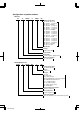
1 INTRODUCTION 1.3 Pins 1.3.1 Pin layout diagram QFP22-256pin 192 129 128 193 INDEX 65 256 1 Pin No. 1 2 3 4 5 6 7 8 9 10 11 12 13 14 15 16 17 18 19 20 21 22 23 24 25 26 27 28 29 30 31 32 33 34 35 36 37 38 39 40 41 42 43 44 45 46 47 48 49 50 51 52 Pin name N.C. N.C.
1 INTRODUCTION 1.3.2 Pin description Table 1.3.2.1 S1C88650 pin description Pin No.
1 INTRODUCTION 1.4 Mask Option Mask options shown below are provided for the S1C88650. Several hardware specifications are prepared in each mask option, and one of them can be selected according to the application. Multiple specifications are available in each option item as indicated in the Option List. Select the specifications that meet the target system and check the appropriate box.
1 INTRODUCTION 5 I/O PORT PULL UP RESISTOR • P00 ......... ■ • P01 ......... ■ • P02 ......... ■ • P03 ......... ■ • P04 ......... ■ • P05 ......... ■ • P06 ......... ■ • P07 ......... ■ • P10 ......... ■ • P11 ......... ■ • P12 ......... ■ • P13 ......... ■ • P14 ......... ■ • P15 ......... ■ • P16 ......... ■ • P17 ......... ■ 1. With Resistor 1. With Resistor 1. With Resistor 1. With Resistor 1. With Resistor 1. With Resistor 1. With Resistor 1. With Resistor 1. With Resistor 1. With Resistor 1.
2 POWER SUPPLY 2 POWER SUPPLY In this section, we will explain the operating voltage and the configuration of the internal power supply circuit of the S1C88650. Either or can be selected as the power source for the LCD system voltage regulator according to the power supply voltage level. 2.1 Operating Voltage The S1C88650 operating power voltage is as follows: 1.8 V to 3.6 V Table 2.2.2 Power source for LCD system voltage regulator 2.
3 CPU AND BUS CONFIGURATION 3 CPU AND BUS CONFIGURATION In this section, we will explain the CPU, operating mode and bus configuration. 3.1 CPU 3.2.2 RAM The S1C88650 utilize the S1C88 8-bit core CPU whose resistor configuration, command set, etc. are virtually identical to other units in the family of processors incorporating the S1C88. The internal RAM capacity is 8K bytes and is allocated to 00D800H–00F7FFH.
3 CPU AND BUS CONFIGURATION 3.3 Exception Processing Vectors 000000H–00004BH in the program area of the S1C88650 is assigned as exception processing vectors. Furthermore, from 00004EH to 0000FFH, software interrupt vectors are assignable to any two bytes which begin with an even address. Table 3.3.1 lists the vector addresses and the exception processing factors to which they correspond. Table 3.3.
3 CPU AND BUS CONFIGURATION When accessing ____ internal memory ____in this mode, _____ the chip enable (CE) and read (RD)/write (WR) signals are not output to external memory, and the data bus (D0–D7) goes into high impedance status (or pull-up status). Consequently, in cases where addresses overlap in external and internal memory, the areas in external memory will be unavailable. 3.5.
3 CPU AND BUS CONFIGURATION - MCU mode - 3.6 External Bus - MPU mode - 3FFFFFH 2FFFFFH External memory area : The S1C88650 has bus terminals that can address a maximum of 1M × 3 bytes and memory (and other) devices can be externally expanded according to the range of each bus mode described in the previous section.
3 CPU AND BUS CONFIGURATION ____ 3.6.2 Address bus The S1C88650 possesses a 20-bit external address bus A0–A19. The terminals and output circuits of address bus A0–A19 are shared with output ports R00–R07 (=A0–A7), R10–R17 (=A8–A15) and R20– R23 (=A16–A19), switching between these functions being determined by the bus mode setting. In the single chip mode, the 20-bit terminals are all set as output ports R00–R07, R10–R17 and R20–R23.
3 CPU AND BUS CONFIGURATION _____ _____ Table 3.6.4.1 CE0–CE2 address settings Address range (expansion mode) MCU mode MPU mode 300000H–3FFFFFH 000000H–00D7FFH, 010000H–0FFFFFH 100000H–1FFFFFH 100000H–1FFFFFH 200000H–2FFFFFH 200000H–2FFFFFH CE signal CE0 CE1 CE2 _____ When accessing the internal memory area, the CE signal is not output. Care should be taken here because the address range for these portions of memory involves irregular settings.
3 CPU AND BUS CONFIGURATION ________ When the bus authority release request (BREQ = LOW) is received from an external device, the____ S1C88650 switches _____ ____ the address bus, data bus, RD/ WR signal, and CE signal lines to a high impedance ________ state, outputs a LOW level from the BACK terminal and releases bus authority. ________ As soon as a LOW level is output from the BACK terminal, the external device can use the external bus.
4 INITIAL RESET 4 INITIAL RESET Initial reset in the S1C88650 is required in order to initialize circuits. This section of the Manual contains a description of initial reset factors and the initial settings for internal registers, etc. ____________ 4.1 Initial Reset Factors 4.1.1 RESET terminal There are two initial reset factors for the S1C88650 as shown below. Initial reset can be_________ done by externally inputting a LOW level to the RESET_________ terminal.
4 INITIAL RESET 4.1.2 Simultaneous LOW level input at input port terminals K00–K03 4.1.3 Initial reset sequence Another way of executing initial reset externally is to input a LOW level simultaneously to the input ports (K00–K03) selected by mask option. Since there is a built-in time authorize circuit, be sure to maintain the designated input port terminal at LOW level for 65536/fOSC1 seconds (two seconds when the oscillation frequency is fOSC1 = 32.
4 INITIAL RESET 4.2 Initial Settings After Initial Reset The CPU internal registers are initialized as follows during initial reset. Table 4.2.
5 PERIPHERAL CIRCUITS AND THEIR OPERATION (I/O Memory Map) 5 PERIPHERAL CIRCUITS AND THEIR OPERATION The peripheral circuits of the S1C88650 is interfaced with the CPU by means of the memory mapped I/O method. For this reason, just as with other memory access operations, peripheral circuits can be controlled by manipulating I/O memory. Below is a description of the operation and control method for each individual peripheral circuit. 5.1 I/O Memory Map Table 5.1.
5 PERIPHERAL CIRCUITS AND THEIR OPERATION (I/O Memory Map) Table 5.1.
5 PERIPHERAL CIRCUITS AND THEIR OPERATION (I/O Memory Map) Table 5.1.
5 PERIPHERAL CIRCUITS AND THEIR OPERATION (I/O Memory Map) Table 5.1.
5 PERIPHERAL CIRCUITS AND THEIR OPERATION (I/O Memory Map) Table 5.1.
5 PERIPHERAL CIRCUITS AND THEIR OPERATION (I/O Memory Map) Table 5.1.
5 PERIPHERAL CIRCUITS AND THEIR OPERATION (I/O Memory Map) Table 5.1.
5 PERIPHERAL CIRCUITS AND THEIR OPERATION (I/O Memory Map) Table 5.1.
5 PERIPHERAL CIRCUITS AND THEIR OPERATION (I/O Memory Map) Table 5.1.
5 PERIPHERAL CIRCUITS AND THEIR OPERATION (I/O Memory Map) Table 5.1.
5 PERIPHERAL CIRCUITS AND THEIR OPERATION (I/O Memory Map) Table 5.1.
5 PERIPHERAL CIRCUITS AND THEIR OPERATION (I/O Memory Map) Table 5.1.
5 PERIPHERAL CIRCUITS AND THEIR OPERATION (I/O Memory Map) Table 5.1.
5 PERIPHERAL CIRCUITS AND THEIR OPERATION (I/O Memory Map) Table 5.1.
5 PERIPHERAL CIRCUITS AND THEIR OPERATION (I/O Memory Map) Table 5.1.
5 PERIPHERAL CIRCUITS AND THEIR OPERATION (I/O Memory Map) Table 5.1.
5 PERIPHERAL CIRCUITS AND THEIR OPERATION (System Controller and Bus Control) 5.2 System Controller and Bus Control The system controller is a management unit which sets such items as the bus mode in accordance with memory system configuration factors.
5 PERIPHERAL CIRCUITS AND THEIR OPERATION (System Controller and Bus Control) _____ _____ Table 5.2.2.1 Address settings of CE0–CE2 Address range (expansion mode) MCU mode MPU mode 300000H–3FFFFFH 000000H–00D7FFH, 010000H–0FFFFFH 100000H–1FFFFFH 100000H–1FFFFFH 200000H–2FFFFFH 200000H–2FFFFFH CE signal CE0 CE1 CE2 _____ The _____ output terminals and output circuits for CE0– CE2 are shared with output ports R30–R32. At initial reset, they are set as output port terminals.
5 PERIPHERAL CIRCUITS AND THEIR OPERATION (System Controller and Bus Control) 5.2.6 Control of system controller Table 5.2.6.1 shows the control bits for the system controller. Table 5.2.6.
5 PERIPHERAL CIRCUITS AND THEIR OPERATION (System Controller and Bus Control) BUSMOD, CPUMOD: 00FF00H•D7, D6 Bus mode and CPU mode are set as shown in Table 5.2.6.2. Table 5.2.6.
5 PERIPHERAL CIRCUITS AND THEIR OPERATION (System Controller and Bus Control) 5.2.7 Programming notes ______ (1) All the interrupts including NMI are masked, until you write the optional value into both the "00FF00H" and "00FF01H" addresses. Consequently, even if you do not change the content of this address (You use the initial value, as is.), you should still be sure to perform the writing operation using the initialization routine.
5 PERIPHERAL CIRCUITS AND THEIR OPERATION (Watchdog Timer) Normally, this routine is integrated at points that are regularly being processed. 5.3 Watchdog Timer 5.3.1 Configuration of watchdog timer The S1C88650 is equipped with a watchdog timer driven by OSC1 as source oscillation. The watchdog timer must be reset periodically by software, and if reset does not take place within the selected period, a non-maskable interrupt signal is generated and output to the CPU.
5 PERIPHERAL CIRCUITS AND THEIR OPERATION (Watchdog Timer) 5.3.3 Control of watchdog timer Table 5.3.3.1 shows the control bits for the watchdog timer. Table 5.3.3.
5 PERIPHERAL CIRCUITS AND THEIR OPERATION (Oscillation Circuits) 5.4.3 OSC1 oscillation circuit 5.4 Oscillation Circuits 5.4.1 Configuration of oscillation circuits The S1C88650 is twin clock system with two internal oscillation circuits (OSC1 and OSC3). The OSC3 oscillation circuit generates the mainclock (Max. 8.2 MHz) to run the CPU and some peripheral circuits in high speed, and the OSC1 oscillation circuit generates the sub-clock (Typ. 32.768 kHz) for low-power operation. Figure 5.4.1.
5 PERIPHERAL CIRCUITS AND THEIR OPERATION (Oscillation Circuits) 5.4.4 OSC3 oscillation circuit The OSC3 oscillation circuit generates the system clock when the CPU and some peripheral circuits are in high speed operation. This oscillation circuit stops when the SLP instruction is executed, or the SOSC3 register is set to "0". In terms of oscillation circuit types, any one of crystal oscillation, ceramic oscillation or CR oscillation can be selected with the mask option. Figure 5.4.4.
5 PERIPHERAL CIRCUITS AND THEIR OPERATION (Oscillation Circuits) 5.4.6 Control of oscillation circuit Table 5.4.6.1 shows the control bits for the oscillation circuits. Table 5.4.6.
5 PERIPHERAL CIRCUITS AND THEIR OPERATION (Input Ports) 5.5.2 Mask option 5.5 Input Ports (K ports) 5.5.1 Configuration of input ports The S1C88650 is equipped with 8 input port bits (K00–K07) all of which are usable as general purpose input port terminals with interrupt function. K04–K07 terminals doubles as the external clock (EXCL0–EXCL3) input terminal of the programmable timer (event counter) with input port functions sharing the input signal as is. (See "5.
5 PERIPHERAL CIRCUITS AND THEIR OPERATION (Input Ports) 5.5.3 Pull-up control 5.5.4 Interrupt function and input comparison register When "With resistor" is selected by mask option, the software can enable and disable the pull-up resistor for each port (1-bit units). The input port with a pull-up resistor suits input from the push switch and key matrix. All the input ports (K00–K07) provide the interrupt functions. The conditions for issuing an interrupt can be set by the software.
5 PERIPHERAL CIRCUITS AND THEIR OPERATION (Input Ports) Table 5.5.4.1 Setting the input level check time CTK02x 1 1 1 1 0 0 0 0 CTK01x 1 1 0 0 1 1 0 0 CTK00x Check time 1 4/fOSC3 0 2/fOSC3 1 1/fOSC3 0 4096/fOSC1 1 2048/fOSC1 0 512/fOSC1 1 128/fOSC1 0 None (∗) (2 µs) (1 µs) (0.5 µs) (128 ms) (64 ms) (16 ms) (4 ms) – ∗: When OSC1 = 32 kHz, OSC3 = 2 MHz Check time setup register CTK00L–CTK02L K00 Input port K00D Notes: • Be sure to disable interrupts before changing the contents of the CTK0x register.
5 PERIPHERAL CIRCUITS AND THEIR OPERATION (Input Ports) 5.5.5 Control of input ports Table 5.5.5.1 shows the input port control bits. Table 5.5.5.
5 PERIPHERAL CIRCUITS AND THEIR OPERATION (Input Ports) Table 5.5.5.
5 PERIPHERAL CIRCUITS AND THEIR OPERATION (Input Ports) KCP00–KCP07: 00FF52H PK00, PK01: 00FF20H•D6, D7 Sets the interrupt generation condition (interrupt generation timing) for input port terminals K00– K07. Sets the input interrupt priority level. PK00 and PK01 are the interrupt priority registers corresponding to the input interrupts. Table 5.5.5.4 shows the interrupt priority level which can be set by this register.
5 PERIPHERAL CIRCUITS AND THEIR OPERATION (Input Ports) 5.5.6 Programming notes (1) When changing the input terminal from LOW level to HIGH with the built-in pull-up resistor, a delay in the waveform rise time will occur depending on the time constant of the pull-up resistor and the load capacitance of the terminal. It is necessary to set an appropriate wait time for introduction of an input port. In particular, special attention should be paid to key scan for key matrix formation.
5 PERIPHERAL CIRCUITS AND THEIR OPERATION (Output Ports) 5.6 Output Ports (R ports) 5.6.1 Configuration of output ports The S1C88650 is equipped with 26 bits of output ports (R00–R07, R10–R17, R20–R25, R30–R33). Depending on the bus mode setting, the configuration of the output ports may vary as shown in the table below. Table 5.6.1.
5 PERIPHERAL CIRCUITS AND THEIR OPERATION (Output Ports) 5.6.4 Control of output ports Table 5.6.4.1 shows the output port control bits. Table 5.6.4.
5 PERIPHERAL CIRCUITS AND THEIR OPERATION (Output Ports) Table 5.6.4.
5 PERIPHERAL CIRCUITS AND THEIR OPERATION (I/O Ports) 5.7 I/O Ports (P ports) 5.7.1 Configuration of I/O ports The S1C88650 is equipped with 16 bits of I/O ports (P00–P07, P10–P17). The configuration of these I/O ports will vary according to the bus mode as shown below. In addition to the general-purpose DC output, special output can be selected for the I/O ports P14–P17 with the software. Table 5.7.1.
5 PERIPHERAL CIRCUITS AND THEIR OPERATION (I/O Ports) Readout in input mode consists simply of a direct readout of the input terminal state: the data being "1" when the input terminal is at HIGH (VDD) level and "0" when it is at LOW (VSS) level. When the built-in pull-up resistor is enabled with the software, the port terminal will be pulled-up to high during input mode. Even in input mode, data can be written to the data registers without affecting the terminal state.
5 PERIPHERAL CIRCUITS AND THEIR OPERATION (I/O Ports) ■ FOUT output (P16) In order for the S1C88650 to provide clock signal to an external device, a FOUT signal (oscillation clock fOSC1 or fOSC3 dividing clock) can be output from the P16 port terminal. The output control for the FOUT signal is done by the register FOUTON. When FOUTON is set to "1", the FOUT signal is output from the P16 port terminal, when "0" is set, the port is set for DC output.
5 PERIPHERAL CIRCUITS AND THEIR OPERATION (I/O Ports) 5.7.6 Control of I/O ports Table 5.7.6.1 shows the I/O port control bits. Table 5.7.6.
5 PERIPHERAL CIRCUITS AND THEIR OPERATION (I/O Ports) Table 5.7.6.
5 PERIPHERAL CIRCUITS AND THEIR OPERATION (I/O Ports) ■ DC output control PULP00–PULP07: 00FF64H PULP10–PULP17: 00FF65H P00D–P07D: 00FF62H P10D–P17D: 00FF63H The pull-up during the input mode are set with these registers. How I/O port terminal Pxx data readout and output data settings are performed.
5 PERIPHERAL CIRCUITS AND THEIR OPERATION (I/O Ports) RPTOUT2: 00FF38H•D4 RPTOUT3: 00FF39H•D4 5.7.7 Programming notes ___________ ___________ Controls the TOUT2/TOUT3 (inverted TOUT2/ TOUT3) signal output. _________ When "1" is written: TOUT signal output When "0" is written: DC output Reading: Valid RPTOUT2 and RPTOUT3 are___________ the output control ___________ registers for the TOUT2 and TOUT3 signals, respectively.
5 PERIPHERAL CIRCUITS AND THEIR OPERATION (Serial Interface) 5.8.2 Switching of terminal functions 5.8 Serial Interface Serial interface input/output _________ _________ 5.8.1 Configuration of serial interface The S1C88650 incorporates a full duplex serial interface (when asynchronous system is selected) that allows the user to select either clock synchronous system or asynchronous system. The data transfer method can be selected in software.
5 PERIPHERAL CIRCUITS AND THEIR OPERATION (Serial Interface) The serial interface terminals are configured according to the transfer mode set using the registers SMD0 and SMD1. SIN and SOUT are serial data input and output terminals which function identically in clock_________ synchronous system and asynchronous system. SCLK is exclusively for use with clock synchronous system and functions as a synchronous clock input/output terminal.
5 PERIPHERAL CIRCUITS AND THEIR OPERATION (Serial Interface) S1C88650 External serial device SIN(P10) Data input SOUT(P11) Data output SCLK(P12) CLOCK input Input port(Kxx) READY output (a) Clock synchronous master mode S1C88650 External serial device SIN(P10) Data input SOUT(P11) Data output SCLK(P12) CLOCK output SRDY(P13) READY input (b) Clock synchronous slave mode S1C88650 External serial device SIN(P10) Data input SOUT(P11) Data output (c) Asynchronous 7-bit/8-bit mode Fig.
5 PERIPHERAL CIRCUITS AND THEIR OPERATION (Serial Interface) 5.8.5 Transmit-receive control Below is a description of the registers which handle transmit-receive control. With respect to transmitreceive control procedures and operations, please refer to the following sections in which these are discussed on a mode by mode basis. ■ Shift register and received data buffer Exclusive shift registers for transmitting and receiving are installed in this serial interface.
5 PERIPHERAL CIRCUITS AND THEIR OPERATION (Serial Interface) 5.8.6 Operation of clock synchronous transfer Clock synchronous transfer involves the transfer of 8-bit data by synchronizing it to eight clocks. The same synchronous clock is used by both the transmitting and receiving sides. When the serial interface is used in the master mode, the clock signal selected using SCS0 and SCS1 is further divided by 1/16 and employed as the synchronous clock.
5 PERIPHERAL CIRCUITS AND THEIR OPERATION (Serial Interface) ■ Data transmit procedure The control procedure and operation during transmitting is as follows. (1) Write "0" in the transmit enable register TXEN and the receive enable register RXEN to reset the serial interface. (2) Write "1" in the transmit enable register TXEN to set into the transmitting enable status. (3) Write the transmitting data into TRXD0– TRXD7.
5 PERIPHERAL CIRCUITS AND THEIR OPERATION (Serial Interface) ■ Data receive procedure The control procedure and operation during receiving is as follows. (1) Write "0" in the receive enable register RXEN and transmit enable register TXEN to reset the serial interface. (2) Write "1" in the receive enable register RXEN to set into the receiving enable status. (3) In case of the master mode, confirm the transmit ready status on the slave side (external serial input/output device), if necessary.
5 PERIPHERAL CIRCUITS AND THEIR OPERATION (Serial Interface) _________ _________ ■ Transmit/receive ready (SRDY) signal When this serial interface is used in the clock synchronous slave mode (external clock input), an _________ SRDY signal is output to indicate whether or not this serial interface can transmit/receive to the master side (external serial input/output device).
5 PERIPHERAL CIRCUITS AND THEIR OPERATION (Serial Interface) 5.8.7 Operation of asynchronous transfer Asynchronous transfer is a mode that transfers by adding a start bit and a stop bit to the front and the back of each piece of serial converted data.
5 PERIPHERAL CIRCUITS AND THEIR OPERATION (Serial Interface) (6) Clock source control When the programmable timer is selected for the clock source, set transfer rate on the programmable timer side. (See "5.10 Programmable Timer".) When the divided signal of OSC3 oscillation circuit is selected for the clock source, be sure that the OSC3 oscillation circuit is turned ON prior to commencing data transfer. (See "5.4 Oscillation Circuits".
5 PERIPHERAL CIRCUITS AND THEIR OPERATION (Serial Interface) ■ Data receive procedure The control procedure and operation during receiving is as follows. (5) Write "1" to the receive control bit RXTRG to inform that the receive data has been read out. When the following data is received prior to writing "1" to RXTRG, it is recognized as an overrun error and the error interrupt factor flag is set to "1".
5 PERIPHERAL CIRCUITS AND THEIR OPERATION (Serial Interface) ■ Receive error During receiving the following three types of errors can be detected by an interrupt. (1) Parity error When writing "1" to the EPR register to select "with parity check", a parity check (vertical parity check) is executed during receiving. After each data bit is sent a parity check bit is sent. The parity check bit is a "0" or a "1". Even parity checking will cause the sum of the parity bit and the other bits to be even.
5 PERIPHERAL CIRCUITS AND THEIR OPERATION (Serial Interface) TXEN TXTRG(RD) TXTRG(WR) Sumpling clock D0 D1 D2 D3 D4 D5 D6 D7 SOUT (In 8-bit mode/Non parity) Interrupt (a) Transmit timing RXEN RXTRG(RD) RXTRG(WR) Sumpling clock SIN D0 D1 D2 D3 D4 D5 D6 D7 (In 8-bit mode/Non parity) TRXD D0 D1 D2 D3 D4 D5 D6 D7 1st data D0 D1 D2 D3 D4 D5 D6 D7 2st data OER control signal OER Interrupt (b) Receive timing Fig. 5.8.7.4 Timing chart (asynchronous transfer, LSB first, stop bit = 1 bit) 5.8.
5 PERIPHERAL CIRCUITS AND THEIR OPERATION (Serial Interface) Address Error generation Address Data bus Address Receive completion Address Address Transmit completion Address Address Interrupt priority register PSIF0, PSIF1 Interrupt factor flag FSERR Interrupt enable register ESERR Interrupt factor flag FSREC Interrupt priority level judgement circuit Interrupt enable register ESREC Interrupt request Interrupt factor flag FSTRA Interrupt enable register ESTRA Fig. 5.8.8.
5 PERIPHERAL CIRCUITS AND THEIR OPERATION (Serial Interface) 5.8.9 Control of serial interface Table 5.8.9.1 show the serial interface control bits. Table 5.8.9.
5 PERIPHERAL CIRCUITS AND THEIR OPERATION (Serial Interface) Table 5.8.9.
5 PERIPHERAL CIRCUITS AND THEIR OPERATION (Serial Interface) SCS0, SCS1: 00FF48H•D3, D4 PMD: 00FF48H•D5 Select the clock source according to Table 5.8.9.3. Selects odd parity/even parity. When "1" is written: Odd parity When "0" is written: Even parity Reading: Valid Table 5.8.9.3 Clock source selection SCS1 1 1 SCS0 1 0 0 0 1 0 Clock source Programmable timer fOSC3 / 4 fOSC3 / 8 fOSC3 / 16 SCS0 and SCS1 can also be read out.
5 PERIPHERAL CIRCUITS AND THEIR OPERATION (Serial Interface) RXTRG: 00FF49H•D3 During receiving Functions as the receiving start trigger or preparation for the following data receiving and the operation status indicator (during receiving/during stop).
5 PERIPHERAL CIRCUITS AND THEIR OPERATION (Serial Interface) FER: 00FF49H•D6 FSTRA, FSREC, FSERR: 00FF27H•D0, D1, D2 Indicates the generation of a framing error. Indicates the serial interface interrupt generation status.
5 PERIPHERAL CIRCUITS AND THEIR OPERATION (Serial Interface) 5.8.10 Programming notes (1) Be sure to initialize the serial interface mode in the transmitting/receiving disable status (TXEN = RXEN = "0"). (2) Do not perform double trigger (writing "1") to TXTRG (RXTRG) when the serial interface is in the transmitting (receiving) operation. Furthermore, do not execute the SLP instruction. (When executing the SLP instruction, set TXEN = RXEN = "0".
5 PERIPHERAL CIRCUITS AND THEIR OPERATION (Clock Timer) 5.9 Clock Timer 5.9.2 Interrupt function 5.9.1 Configuration of clock timer The clock timer can generate an interrupt by each of the 32 Hz, 8 Hz, 2 Hz and 1 Hz signals. The configuration of the clock timer interrupt circuit is shown in Figure 5.9.2.1. The S1C88650 has built in a clock timer that uses the OSC1 oscillation circuit as clock source.
5 PERIPHERAL CIRCUITS AND THEIR OPERATION (Clock Timer) Address 32 Hz falling edge Address Address 8 Hz falling edge Data bus Address Address 2 Hz falling edge Address Address 1 Hz falling edge Address Address Interrupt priority register PTM0, PTM1 Interrupt factor flag FTM32 Interrupt enable register ETM32 Interrupt factor flag FTM8 Interrupt enable register ETM8 Interrupt priority level judgement circuit Interrupt request Interrupt factor flag FTM2 Interrupt enable register ETM2 Interrupt
5 PERIPHERAL CIRCUITS AND THEIR OPERATION (Clock Timer) 5.9.3 Control of clock timer Table 5.9.3.1 shows the clock timer control bits. Table 5.9.3.
5 PERIPHERAL CIRCUITS AND THEIR OPERATION (Clock Timer) TMD0–TMD7: 00FF41H ETM1, ETM2, ETM8, ETM32: 00FF22H•D0–D3 The clock timer data can be read out. Each bit of TMD0–TMD7 and frequency correspondence are as follows: Enables or disables the generation of an interrupt for the CPU.
5 PERIPHERAL CIRCUITS AND THEIR OPERATION (Clock Timer) 5.9.4 Programming notes (1) The clock timer is actually made to RUN/STOP in synchronization with the falling edge of the 256 Hz signal after writing to the TMRUN register. Consequently, when "0" is written to the TMRUN, the timer shifts to STOP status when the counter is incremented "1". The TMRUN maintains "1" for reading until the timer actually shifts to STOP status. Figure 5.9.4.1 shows the timing chart of the RUN/STOP control.
5 PERIPHERAL CIRCUITS AND THEIR OPERATION (Programmable Timer) 5.10 Programmable Timer 5.10.1 Configuration of programmable timer The S1C88650 has four built-in 16-bit programmable timer systems. Each system timer consists of a 16-bit presettable down counter, and can be used as 16-bit × 1 channel or 8-bit × 2 channels of programmable timer. Furthermore, they function as event counters using the input port terminal. Figures 5.10.1.1 and 5.10.1.2 shows the configuration of the 16-bit programmable timers.
5 PERIPHERAL CIRCUITS AND THEIR OPERATION (Programmable Timer) fOSC3/fOSC1 Input port (K06) Prescaler/clock control circuit INCL4 EXCL2 Timer 4 Clock selection circuit 8-bit reload data register (RDR4) 8-bit down counter (PTM4) Underflow Underflow interrupt Compare match interrupt Comparator Interrupt circuit Control circuit Compare match 8-bit compare data register (CDR4) Timer 4 control registers Underflow signal Prescaler/clock control circuit INCL5 EXCL2 8-bit reload data register (RDR5) 8
5 PERIPHERAL CIRCUITS AND THEIR OPERATION (Programmable Timer) [8-bit mode] [16-bit mode] 8-bit data Low-order 8-bit data Timer 0 input clock Timer 0 Interrupt request TOUT output Timer 0 input clock Timer 0 Timer 1 input clock Timer 1 Interrupt request TOUT output Timer 0 underflow signal Timer 1 8-bit data Interrupt request TOUT output High-order 8-bit data Fig. 5.10.2.1 Counter configuration in 8- and 16-bit mode (example of Timers 0 and 1) Table 5.10.2.
5 PERIPHERAL CIRCUITS AND THEIR OPERATION (Programmable Timer) 5.10.3 Setting of input clock Table 5.10.3.2 Division ratio and control registers The clock to be input to the counter can be selected from either the internal clock or external clock by the input clock selection register (CKSEL) provided for each timer. The internal clock is an output of the prescaler. The external clock is used for the event counter function. A signal from the input port is used as the count clock. Table 5.10.3.
5 PERIPHERAL CIRCUITS AND THEIR OPERATION (Programmable Timer) Compare data register The programmable timer has a built-in data comparator so that count data can be compared with an optional value. The compare data register (CDRx) is used to set the value to be compared. In the 8-bit mode, CDRx is used as an 8-bit register separated for each timer. In the 16-bit mode, the CDR(L) register is handled as low-order 8 bits of compare data, and the CDR(H) register is as high-order 8 bits.
5 PERIPHERAL CIRCUITS AND THEIR OPERATION (Programmable Timer) In the 16-bit mode, the interrupt factor flags of Timer(H) are set to "1" by the compare match and underflow in 16 bits. 5.10.5 Interrupt function The 16-bit programmable timer can generate an interrupt with the compare match signal and underflow signal of each timer. Figure 5.10.5.1 shows the configuration of the 16bit programmable timer interrupt circuit. Refer to Section 5.
5 PERIPHERAL CIRCUITS AND THEIR OPERATION (Programmable Timer) Address Underflow Address Address Compare match Address Address Address Underflow Address Address Compare match Data bus Address Address Address Underflow Address Address Compare match Address Address Address Underflow Address Address Compare match Address Address Interrupt priority register PPT0, PPT1 Interrupt factor flag FTU0 Interrupt enable register ETU0 Interrupt priority level judgment circuit Interrupt factor fla
5 PERIPHERAL CIRCUITS AND THEIR OPERATION (Programmable Timer) 5.10.6 Setting of TOUT output The 16-bit programmable timer can generate TOUT signals with the underflow and compare match signals of each timer. The TOUT signal generated in the 16-bit programmable timer can be output from the I/O port terminal shown in Table 5.10.6.1 so that a clock is supplied for external devices or it can be used as a PWM waveform output. Table 5.10.6.
5 PERIPHERAL CIRCUITS AND THEIR OPERATION (Programmable Timer) 5.10.7 Transfer rate setting of serial interface The underflow signal of Timer 1 can be used to clock the serial interface. The transfer rate setting in this case is made in the registers PST1X and RDR1X (since only the underflow signal is used as the serial interface clock source, the CDR1X register value does not affect the transfer rates. It can be set to any value).
5 PERIPHERAL CIRCUITS AND THEIR OPERATION (Programmable Timer) 5.10.9 Control of programmable timer Table 5.10.9.1 shows the programmable timer control bits. Table 5.10.9.
5 PERIPHERAL CIRCUITS AND THEIR OPERATION (Programmable Timer) Table 5.10.9.
5 PERIPHERAL CIRCUITS AND THEIR OPERATION (Programmable Timer) Table 5.10.9.
5 PERIPHERAL CIRCUITS AND THEIR OPERATION (Programmable Timer) Table 5.10.9.
5 PERIPHERAL CIRCUITS AND THEIR OPERATION (Programmable Timer) Table 5.10.9.
5 PERIPHERAL CIRCUITS AND THEIR OPERATION (Programmable Timer) Table 5.10.9.
5 PERIPHERAL CIRCUITS AND THEIR OPERATION (Programmable Timer) Table 5.10.9.
5 PERIPHERAL CIRCUITS AND THEIR OPERATION (Programmable Timer) Table 5.10.9.
5 PERIPHERAL CIRCUITS AND THEIR OPERATION (Programmable Timer) MODE16_A: 00FF30H•D7 MODE16_B: 00FF38H•D7 MODE16_C: 00FFB0H•D7 MODE16_D: 00FFB8H•D7 Selects either the 8/16 bit mode. When "1" is written: 16 bits × 1 channel When "0" is written: 8 bits × 2 channels Reading: Valid MODE16_A, MODE16_B, MODE16_C and MODE16_D are the 8/16-bit mode selection registers corresponding to Timers 0 and 1, Timers 2 and 3, Timers 4 and 5, and Timers 6 and 7, respectively.
5 PERIPHERAL CIRCUITS AND THEIR OPERATION (Programmable Timer) PRPRT0: 00FF14H•D3 PRPRT1: 00FF14H•D7 PRPRT2: 00FF15H•D3 PRPRT3: 00FF15H•D7 PRPRT4: 00FF18H•D3 PRPRT5: 00FF18H•D7 PRPRT6: 00FF19H•D3 PRPRT7: 00FF19H•D7 PTM00–PTM07: 00FF36H PTM10–PTM17: 00FF37H PTM20–PTM27: 00FF3EH PTM30–PTM37: 00FF3FH PTM40–PTM47: 00FFB6H PTM50–PTM57: 00FFB7H PTM60–PTM67: 00FFBEH PTM70–PTM77: 00FFBFH Controls the clock supply of each timer (when internal clock is used). The counter data of each timer can be read.
5 PERIPHERAL CIRCUITS AND THEIR OPERATION (Programmable Timer) PTRUN0: 00FF30H•D2 PTRUN1: 00FF31H•D2 PTRUN2: 00FF38H•D2 PTRUN3: 00FF39H•D2 PTRUN4: 00FFB0H•D2 PTRUN5: 00FFB1H•D2 PTRUN6: 00FFB8H•D2 PTRUN7: 00FFB9H•D2 RPTOUT2: 00FF38H•D4 RPTOUT3: 00FF39H•D4 _________ Controls the output of the TOUT signal. _________ When "1" is written: TOUT signal output When "0" is written: DC output Reading: Valid Controls the RUN/STOP of the counter.
5 PERIPHERAL CIRCUITS AND THEIR OPERATION (Programmable Timer) ETU0: 00FF25H•D0 ETU1: 00FF25H•D2 ETU2: 00FF25H•D4 ETU3: 00FF25H•D6 ETU4: 00FF2CH•D0 ETU5: 00FF2CH•D2 ETU6: 00FF2CH•D4 ETU7: 00FF2CH•D6 FTU0: 00FF29H•D0 FTU1: 00FF29H•D2 FTU2: 00FF29H•D4 FTU3: 00FF29H•D6 FTU4: 00FF2EH•D0 FTU5: 00FF2EH•D2 FTU6: 00FF2EH•D4 FTU7: 00FF2EH•D6 Enables or disables the underflow interrupt generation to the CPU. Indicates the generation of underflow interrupt factor.
5 PERIPHERAL CIRCUITS AND THEIR OPERATION (Programmable Timer) FTCx is the interrupt factor flag corresponding to interrupt of Timer x, and is set to "1" with the compare match signal. At this point, if the corresponding interrupt enable register is set to "1" and the corresponding interrupt priority register is set to a higher level than the setting of the interrupt flags (I0 and I1), an interrupt is generated to the CPU.
5 PERIPHERAL CIRCUITS AND THEIR OPERATION (LCD Driver) 5.11.2 LCD power supply 5.11 LCD Driver 5.11.1 Configuration of LCD driver The S1C88650 has a built-in dot matrix LCD driver that can drive an LCD panel with a maximum of 4,032 dots (126 segments × 32 commons). Figure 5.11.1.1 shows the configuration of the LCD driver and the drive power supply. The S1C88650 generates the LCD drive voltages VC1 to VC5 using the internal power supply circuit. It is not necessary to apply an external voltage.
5 PERIPHERAL CIRCUITS AND THEIR OPERATION (LCD Driver) 5.11.3 Frame frequency 5.11.4 Switching drive duty This LCD driver allows selection of the source clock for generating the frame signal from the OSC1 oscillation clock (fOSC1) and the programmable timer 5 underflow signal. By using programmable timer 5, flexible frame frequencies can be programmed. Refer to Section 5.10.8, "Setting frame frequency for LCD driver".
5 PERIPHERAL CIRCUITS AND THEIR OPERATION (LCD Driver) 32 Hz* 0 1 2 3 – – 31 0 1 2 3 – – 31 VDD VSS COM0 VC5 VC4 VC3 VC2 VC1 VSS ~ ~ ~ ~ ~ ~ COM0 1 2 3 4 5 6 7 FR COM1 ~ ~ ~ ~ 8 9 10 11 12 13 14 15 ~ ~ VC5 VC4 VC3 VC2 VC1 VSS ~ ~ VC5 VC4 VC3 VC2 VC1 VSS ~ ~ COM0–SEG1 VC5 VC4 VC3 VC2 VC1 VSS VC5 VC4 VC3 VC2 VC1 VSS (GND) -VC1 -VC2 -VC3 -VC4 -VC5 ~ ~ SEG0 1 2 3 4 COM0–SEG0 ~ ~ SEG1 24 25 26 27 28 29 30 31 ~ ~ SEG0 ~ ~ 16 17 18 19 20 21 22 23 ~ ~ ~ ~ COM2 VC5 VC4 VC3 VC2 VC1
5 PERIPHERAL CIRCUITS AND THEIR OPERATION (LCD Driver) 32 Hz* 0 1 2 3 – – 15 0 1 2 3 – – 15 VDD VSS COM0 VC5 VC4 VC3 VC2 VC1 VSS ~ ~ ~ ~ ~ ~ COM0 1 2 3 4 5 6 7 FR COM1 ~ ~ ~ ~ 8 9 10 11 12 13 14 15 ~ ~ ~ ~ ~ ~ VC5 VC4 VC3 VC2 VC1 VSS VC5 VC4 VC3 VC2 VC1 VSS ~ ~ COM0–SEG1 VC5 VC4 VC3 VC2 VC1 VSS VC5 VC4 VC3 VC2 VC1 VSS (GND) -VC1 -VC2 -VC3 -VC4 -VC5 ~ ~ COM0–SEG0 ~ ~ SEG1 ~ ~ SEG0 ~ ~ SEG0 1 2 3 4 ~ ~ COM2 VC5 VC4 VC3 VC2 VC1 VSS VC5 VC4 VC3 VC2 VC1 VSS (GND) -VC1 -VC2 -VC3 -V
5 PERIPHERAL CIRCUITS AND THEIR OPERATION (LCD Driver) 64 Hz* 0 1 2 3 4 5 6 7 0 1 2 3 4 5 6 7 SEG0 1 2 3 4 COM0 1 2 3 4 5 6 7 FR VDD VSS COM0 VC5 VC4 VC3 VC2 VC1 VSS COM1 VC5 VC4 VC3 VC2 VC1 VSS COM2 VC5 VC4 VC3 VC2 VC1 VSS SEG0 VC5 VC4 VC3 VC2 VC1 VSS SEG1 VC5 VC4 VC3 VC2 VC1 VSS COM0–SEG0 VC5 VC4 VC3 VC2 VC1 VSS (GND) -VC1 -VC2 -VC3 -VC4 -VC5 COM0–SEG1 VC5 VC4 VC3 VC2 VC1 VSS (GND) -VC1 -VC2 -VC3 -VC4 -VC5 ∗ when fOSC1 (32.768 kHz) is selected as the source clock (FRMCS = "0") Fig. 5.
5 PERIPHERAL CIRCUITS AND THEIR OPERATION (LCD Driver) The memory allocation for the SEG terminals can be reversed using the SEG assignment reverse register SEGREV. 5.11.5 Display memory The S1C88650 has a built-in 768-byte display memory. The display memory is allocated to address Fx00H–Fx7FH (x = 8–DH) and the correspondence between the memory bits and common/segment terminal is changed according to the selection status of the following items. Table 5.11.5.
5 PERIPHERAL CIRCUITS AND THEIR OPERATION (LCD Driver) 0 1 2 Address / 0–F 0–F 0–F Data bit D0 D1 00F800H D2 D3 | D4 00F87DH D5 D6 D7 D0 D1 00F900H D2 D3 | D4 00F97DH D5 D6 D7 D0 D1 00FA00H D2 D3 | D4 00FA7DH D5 D6 D7 D0 D1 00FB00H D2 D3 | D4 00FB7DH D5 D6 D7 D0 D1 00FC00H D2 D3 | D4 00FC7DH D5 D6 D7 D0 D1 00FD00H D2 D3 | D4 00FD7DH D5 D6 D7 SEG (normal)*1 0–15 16–31 32–47 SEG (reverse)*2 125–112 111–96 95–80 ∗1: SEGREV = "0" ∗2: SEGREV = "1" 3 0–F 4 0–F 5 0–F 6 0–F 7 0–D 0 1 2 3 4 5 6 7 8 9 10 11 12
5 PERIPHERAL CIRCUITS AND THEIR OPERATION (LCD Driver) 0 1 2 Address / 0–F 0–F 0–F Data bit D0 D1 00F800H D2 D3 | D4 00F87DH D5 D6 D7 D0 D1 00F900H D2 D3 | D4 00F97DH D5 D6 D7 D0 D1 00FA00H D2 D3 | D4 00FA7DH D5 D6 D7 D0 D1 00FB00H D2 D3 | D4 00FB7DH D5 D6 D7 D0 D1 00FC00H D2 D3 | D4 00FC7DH D5 D6 D7 D0 D1 00FD00H D2 D3 | D4 00FD7DH D5 D6 D7 SEG (normal)*1 0–15 16–31 32–47 SEG (reverse)*2 125–112 111–96 95–80 ∗1: SEGREV = "0" ∗2: SEGREV = "1" 3 0–F 4 0–F 5 0–F 6 0–F 7 0–D COM Display area 0 1 2 3 4
5 PERIPHERAL CIRCUITS AND THEIR OPERATION (LCD Driver) 0 1 2 3 4 5 6 7 Address / COM 0–F 0–F 0–F 0–F 0–F 0–F 0–F 0–D Data bit D0 0 D1 1 D2 2 00F800H D3 3 | Display area 0 (when DSPAR is set to "0") D4 4 5 00F87DH D5 D6 6 D7 7 D0 8 D1 9 10 00F900H D2 D3 11 | Display area 0 (when DSPAR is set to "0") 12 D4 13 00F97DH D5 14 D6 15 D7 D0 0 D1 1 2 00FA00H D2 D3 3 | Display area 1 (when DSPAR is set to "1") D4 4 5 00FA7DH D5 6 D6 7 D7 D0 8 D1 9 10 00FB00H D2 D3 11 | Display area 1 (when DSPAR is set to "1") D4 12
5 PERIPHERAL CIRCUITS AND THEIR OPERATION (LCD Driver) 0 1 2 3 4 5 6 7 Address / COM 0–F 0–F 0–F 0–F 0–F 0–F 0–F 0–D Data bit D0 0 D1 1 D2 2 00F800H D3 3 | D4 4 5 00F87DH D5 Display area 0 (when DSPAR is set to "0") D6 6 D7 7 D0 8 D1 9 10 00F900H D2 D3 11 | D4 00F97DH D5 D6 D7 D0 12 D1 13 Display area 0 (when DSPAR is set to "0") 14 00FA00H D2 D3 15 | D4 00FA7DH D5 D6 D7 D0 0 D1 1 2 00FB00H D2 D3 3 | D4 4 5 00FB7DH D5 Display area 1 (when DSPAR is set to "1") D6 6 D7 7 D0 8 D1 9 D2 10 00FC00H D3 11 | D4 00
5 PERIPHERAL CIRCUITS AND THEIR OPERATION (LCD Driver) 0 1 2 3 4 5 6 7 Address / COM 0–F 0–F 0–F 0–F 0–F 0–F 0–F 0–D Data bit D0 0 D1 1 D2 2 00F800H D3 3 | Display area 0 (when DSPAR is set to "0") D4 4 5 00F87DH D5 D6 6 D7 7 D0 D1 00F900H D2 D3 | D4 00F97DH D5 D6 D7 D0 0 D1 1 2 00FA00H D2 D3 3 | Display area 1 (when DSPAR is set to "1") D4 4 5 00FA7DH D5 D6 6 D7 7 D0 D1 00FB00H D2 D3 | D4 00FB7DH D5 D6 D7 D0 D1 00FC00H D2 D3 | D4 00FC7DH D5 D6 D7 D0 D1 00FD00H D2 D3 | D4 00FD7DH D5 D6 D7 SEG (normal)*1 0–
5 PERIPHERAL CIRCUITS AND THEIR OPERATION (LCD Driver) 0 1 2 3 4 5 6 7 Address / COM 0–F 0–F 0–F 0–F 0–F 0–F 0–F 0–D Data bit D0 0 D1 1 D2 2 00F800H D3 3 | Display area 0 (when DSPAR is set to "0") D4 4 5 00F87DH D5 D6 6 D7 7 D0 D1 00F900H D2 D3 | D4 00F97DH D5 D6 D7 D0 D1 00FA00H D2 D3 | D4 00FA7DH D5 D6 D7 D0 0 D1 1 2 00FB00H D2 D3 3 | Display area 1 (when DSPAR is set to "1") D4 4 5 00FB7DH D5 D6 6 D7 7 D0 D1 00FC00H D2 D3 | D4 00FC7DH D5 D6 D7 D0 D1 00FD00H D2 D3 | D4 00FD7DH D5 D6 D7 SEG (normal)*1 0–
5 PERIPHERAL CIRCUITS AND THEIR OPERATION (LCD Driver) 5.11.6 Display control The display status of the built-in LCD driver and the contrast adjustment can be controlled with the built-in LCD driver. The LCD display status can be selected by display control registers LCDC0 and LCDC1. Setting the value and display status are shown in Table 5.11.6.1. Table 5.11.6.
5 PERIPHERAL CIRCUITS AND THEIR OPERATION (LCD Driver) 5.11.7 Control of LCD driver Table 5.11.7.1 shows the LCD driver control bits. Table 5.11.7.
5 PERIPHERAL CIRCUITS AND THEIR OPERATION (LCD Driver) DTFNT: 00FF10H•D2 LCDC0, LCDC1: 00FF11H•D4, D5 Selects the dot font. Controls the LCD display. When "1" is written: 12 × 12 dots When "0" is written: 16 × 16/5 × 8 dots Reading: Valid Select 16 × 16/5 × 8 dots or 12 × 12 dots type for the display memory area. When "0" is written to DTFNT, 16 × 16/5 × 8 dots is selected and when "1" is written, 12 × 12 dots is selected.
5 PERIPHERAL CIRCUITS AND THEIR OPERATION (LCD Driver) DBON: 00FF03H•D0 5.11.8 Programming notes Control the power voltage booster circuit. (1) When the SLP instruction is executed, display control registers LCDC0 and LCDC1 are automatically reset to "0" by hardware. When "1" is written: ON When "0" is written: OFF Reading: Valid When "1" is written to DBON, the power voltage booster activates and almost doubles the VDD voltage to generate the VD2 voltage.
5 PERIPHERAL CIRCUITS AND THEIR OPERATION (SVD Circuit) Table 5.12.2.1 Criteria voltage setting 5.12 Supply Voltage Detection (SVD) Circuit 5.12.1 Configuration of SVD circuit The S1C88650 has a built-in SVD (supply voltage detection) circuit, so that the software can find when the source voltage lowers. Turning the SVD circuit ON/OFF and the SVD criteria voltage setting can be done with software. Figure 5.12.1.1 shows the configuration of the SVD circuit. 5.12.
5 PERIPHERAL CIRCUITS AND THEIR OPERATION (SVD Circuit) 5.12.3 Control of SVD circuit Table 5.12.3.1 shows the SVD circuit control bits. Table 5.12.3.
5 PERIPHERAL CIRCUITS AND THEIR OPERATION (Heavy Load Protection Function) 5.13 Heavy Load Protection Function 5.13.1 Outline of heavy load protection function The S1C88650 has a heavy load protection function to prevent malfunction due to a power voltage fluctuation caused by a heavy battery load such as when an external lamp is driven and while the IC is running in high-speed with the OSC3 clock. This function works when the IC enters the heavy load protection mode.
5 PERIPHERAL CIRCUITS AND THEIR OPERATION (Interrupt and Standby Status) 5.14.1 Interrupt generation conditions 5.14 Interrupt and Standby Status The interrupt factor flags that indicate the generation of their respective interrupt factors are provided for the previously indicated 4 systems and 31 types of interrupts and they will be set to "1" by the generation of a factor. In addition, interrupt enable registers with a 1 to 1 correspondence to each of the interrupt factor flags are provided.
Interrupt factor flag Interrupt enable register Interrupt priority register K07 K06 K05 K04 Input port K03 K02 K01 K00 Programmable timer 0 Programmable timer 1 Programmable timer 2 Programmable timer 3 Programmable timer 4 Programmable timer 5 Programmable timer 6 Programmable timer 7 Underflow Compare match Underflow Compare match Underflow Compare match Underflow Compare match Underflow Compare match Underflow Compare match Underflow Compare match Underflow Compare match Error Serial interface
5 PERIPHERAL CIRCUITS AND THEIR OPERATION (Interrupt and Standby Status) 5.14.2 Interrupt factor flag Table 5.14.2.1 shows the correspondence between the factors generating an interrupt and the interrupt factor flags. The corresponding interrupt factor flags are set to "1" by generation of the respective interrupt factors. The corresponding interrupt factor can be confirmed by reading the flags through software. Interrupt factor flag that has been set to "1" is reset to "0" by writing "1".
5 PERIPHERAL CIRCUITS AND THEIR OPERATION (Interrupt and Standby Status) 5.14.3 Interrupt enable register The interrupt enable register has a 1 to 1 correspondence with each interrupt factor flag and enable/disable of interrupt requests can be set. When "1" is written to the interrupt enable register, an interrupt request is enabled, and is disabled when "0" is written. This register also permits reading, thus making it possible to confirm that a status has been set.
5 PERIPHERAL CIRCUITS AND THEIR OPERATION (Interrupt and Standby Status) 5.14.4 Interrupt priority register and interrupt priority level Table 5.14.4.
5 PERIPHERAL CIRCUITS AND THEIR OPERATION (Interrupt and Standby Status) Table 5.14.5.1 Vector address and exception processing correspondence 5.14.5 Exception processing vectors When the CPU accepts an interrupt request, it starts exception processing following completion of the instruction being executed. In exception processing, the following operations branch the program.
5 PERIPHERAL CIRCUITS AND THEIR OPERATION (Interrupt and Standby Status) 5.14.6 Control of interrupt Table 5.14.6.1 shows the interrupt control bits. Table 5.14.6.
5 PERIPHERAL CIRCUITS AND THEIR OPERATION (Interrupt and Standby Status) Table 5.14.6.
5 PERIPHERAL CIRCUITS AND THEIR OPERATION (Interrupt and Standby Status) Table 5.14.6.
6 SUMMARY OF NOTES 6 SUMMARY OF NOTES 6.1 Notes for Low Current Consumption The S1C88650 can turn circuits, which consume a large amount of power, ON or OFF by control registers. You can reduce power consumption by creating a program that operates the minimum necessary circuits using these control registers. Next, which circuit systems' operation can be controlled and their control registers (instructions) are explained. You should refer to these when programming.
6 SUMMARY OF NOTES 6.2 Precautions on Mounting ● Oscillation characteristics change depending on conditions (board pattern, components used, etc.). In particular, when a ceramic or crystal oscillator is used, use the oscillator manufacturer's recommended values for constants such as capacitance and resistance. ● Sudden power supply variation due to noise may cause malfunction.
6 SUMMARY OF NOTES ● Visible radiation causes semiconductor devices to change the electrical characteristics. It may cause this IC to malfunction. When developing products which use this IC, consider the following precautions to prevent malfunctions caused by visible radiations. (1) Design the product and implement the IC on the board so that it is shielded from visible radiation in actual use.
7 BASIC EXTERNAL WIRING DIAGRAM 7 BASIC EXTERNAL WIRING DIAGRAM ∗1 RCR1 CG1 OSC1 COM31 ∗2 COM0 VSS SEG125 SEG0 LCD panel 126 x 32 K00–K02 K03 (BREQ) X'tal1 ∗4 ∗3 RCR3 CG2 X'tal2 or Ceramic CD2 OSC2 K04–K07 OSC3 Rf C1 C2 C3 C4 C5 C6 C7 C8 C9 C10 C11 OSC4 VD1 R00–R07 (A0–A7) R10–R17 (A8–A15) VC1 VC2 VC3 VC4 VC5 CA CB CC CD S1C88650 R30–R32 (CE0–CE2) R33 (BACK) [The potential of the substrate (back of the chip) is VSS.
8 ELECTRICAL CHARACTERISTICS 8 ELECTRICAL CHARACTERISTICS 8.1 Absolute Maximum Rating Item Output voltage High level output current Symbol Condition VDD VC5 VI VO IOH 1 terminal Low level output current IOL Permitted loss PD Topr Tstg Power voltage Liquid crystal power voltage Input voltage Total of all terminals 1 terminal Total of all terminals Operating temperature Storage temperature Soldering temperature / time Note) 1 In case of plastic package. (VSS = 0 V) Unit Note V V V Rated value -0.
8 ELECTRICAL CHARACTERISTICS 8.3 DC Characteristics Unless otherwise specified: VDD = 1.8 to 3.
8 ELECTRICAL CHARACTERISTICS 8.4 Analog Circuit Characteristics ■ LCD drive circuit The typical values in the following LCD driver characteristics varies depending on the panel load (panel size, number of display pixels and display contents), so evaluate them by connecting to the actually used LCD panel. Refer to Section 8.8, "Characteristics Curves" for the load characteristic. Unless otherwise specified: VDD = 1.8 to 3.6 V, VSS = 0 V, Ta = 25°C, C1–C11 = 0.
8 ELECTRICAL CHARACTERISTICS 8.5 Power Current Consumption Unless otherwise specified: VDD = 1.8 to 3.6 V, VSS = 0 V, Ta = 25°C, C1–C11 = 0.1 µF, No panel load Item Symbol Condition Min. Typ. Max. Unit Note Current consumption in SLEEP mode Current consumption in HALT mode Current consumption during execution Current consumption during execution in heavy load protection mode LCD circuit current 1 2.5 µA 2.
8 ELECTRICAL CHARACTERISTICS 8.6 AC Characteristics ■ Operating range Condition: VDD = 1.8 to 3.6 V, VSS = 0 V, Ta = -20 to 70°C Item Symbol Condition fOSC1 VDD = 1.8 to 3.
8 ELECTRICAL CHARACTERISTICS ■ External memory access • Read cycle Condition: VDD = 1.8 to 3.6 V, VSS = 0 V, Ta = 25°C, VIH1 = 0.8VDD, VIL1 = 0.2VDD, VIH2 = 1.6 V, VIL2 = 0.6 V, VOH = 0.8VDD, VOL = 0.2VDD, CL = 100 pF (load capacitance) Item Symbol Min. Typ. Max.
8 ELECTRICAL CHARACTERISTICS ■ Serial interface • Clock synchronous master mode Condition: VDD = 1.8 to 3.6 V, VSS = 0 V, Ta = 25°C, VIH1 = 0.8VDD, VIL1 = 0.2VDD, VOH = 0.8VDD, VOL = 0.2VDD Item Symbol Min. Typ. Max. 100 Transmitting data output delay time tsmd tsms 250 Receiving data input set-up time tsmh 100 Receiving data input hold time Unit Note ns ns ns • Clock synchronous slave mode Condition: VDD = 1.8 to 3.6 V, VSS = 0 V, Ta = 25°C, VIH1 = 0.8VDD, VIL1 = 0.2VDD, VOH = 0.8VDD, VOL = 0.
8 ELECTRICAL CHARACTERISTICS ■ Input clock _________ • SCLK, EXCL input clock Condition: VDD = 1.8 to 3.6 V, VSS = 0 V, Ta = 25°C, VIH1 = 0.8VDD, VIL1 = 0.2VDD Item Symbol Min. Typ.
8 ELECTRICAL CHARACTERISTICS ■ Power ON reset using an external capacitor Condition: VDD = 1.8 to 3.6 V, VSS = 0 V, Ta = 25°C Item Symbol Min. Typ. Max. Unit Note Operating power voltage Vsr 1.8 V RESET input time tpsr 10 ms Vsr VDD tpsr 0.5VDD RESET 0.1VDD Power ON VDD *1 RESET VSS *1 Because the potential of the RESET terminal not reached VDD level or higher.
8 ELECTRICAL CHARACTERISTICS 8.7 Oscillation Characteristics Oscillation characteristics change depending on conditions (board pattern, components used, etc.). Use the following characteristics as reference values. In particular, when a ceramic oscillator or crystal oscillator is used for OSC3, use the oscillator manufacturer’s recommended values for constants such as capacitance and resistance. The oscillation start time is important because it becomes the wait time when OSC3 clock is used.
8 ELECTRICAL CHARACTERISTICS 8.8 Characteristics Curves (reference value) ■ High level output current-voltage characteristic Ta = 70°C, Max. value VDD–VOH [V] 0.0 0 0.2 0.4 0.6 0.8 1.0 IOH [mA] -3 -6 VDD = 1.8 V -9 -12 VDD = 3.6 V VDD = 2.4 V -15 ■ Low level output current-voltage characteristic Ta = 70°C, Min. value 15 VDD = 3.6 V VDD = 1.8 V VDD = 2.4 V IOL [mA] 12 9 6 3 0 0.0 150 0.1 0.2 0.3 VOL [V] EPSON 0.4 0.5 0.
8 ELECTRICAL CHARACTERISTICS ■ LCD drive voltage-supply voltage characteristic (when the power voltage booster is not used) Connects 1 MΩ load resistor between VSS and VC5. (no panel load) Ta = 25°C, Typ. value 7.0 VC5 [V] 6.0 LCx = FH 5.0 LCx = 0H 4.0 3.0 2.0 1.5 2.0 2.5 3.0 3.5 4.0 VDD [V] ■ LCD drive voltage-supply voltage characteristic (when the power voltage booster is used) Connects 1 MΩ load resistor between VSS and VC5. (no panel load) Ta = 25°C, Typ. value 7.0 VC5 [V] 6.
8 ELECTRICAL CHARACTERISTICS ■ LCD drive voltage-ambient temperature characteristic Typ. value 1.05VC5 1.04VC5 1.03VC5 VC5 [V] 1.02VC5 1.01VC5 1.00VC5 0.99VC5 0.98VC5 0.97VC5 0.96VC5 0.95VC5 -50 -25 0 25 Ta [°C] 50 75 100 ■ LCD drive voltage-load characteristic Ta = 25°C, Typ. value, LCx = 8H 5.30 5.25 5.20 VC5 [V] 5.15 5.10 5.05 5.00 4.95 4.
8 ELECTRICAL CHARACTERISTICS ■ SVD voltage-ambient temperature characteristic Typ. value, SVDSx = FH 1.05VSVD 1.04VSVD 1.03VSVD VSVD [V] 1.02VSVD 1.01VSVD 1.00VSVD 0.99VSVD 0.98VSVD 0.97VSVD 0.96VSVD 0.
8 ELECTRICAL CHARACTERISTICS ■ In HALT status current consumption temperature characteristic (During operation with OSC1) Typ. value 8 IHALT1 [µA] 6 4 2 0 -50 -25 0 25 Ta [°C] 50 75 100 ■ In HALT status current consumption resistor characteristic (During operation with OSC1) Ta = 25°C 60 50 IHALT2 [µA] 40 30 20 Max. 10 0 100 154 Typ.
8 ELECTRICAL CHARACTERISTICS ■ In executed status current consumption temperature characteristic (During operation with OSC1) Typ. value 16 IEXE1 [µA] 12 8 4 0 -50 -25 0 25 Ta [°C] 50 75 100 ■ In executed status current consumption resistor characteristic (During operation with OSC1) Ta = 25°C 160 140 IEXE2 [µA] 120 100 80 60 40 Max. 20 Typ.
8 ELECTRICAL CHARACTERISTICS ■ In executed status current consumption frequency characteristic (During operation with OSC3) Ta = 25°C 4000 Max. 3500 IEXE3 [µA] 3000 2500 2000 Typ. 1500 1000 500 0 0.0 2.0 4.0 6.0 8.0 10.0 fOSC3 [MHz] ■ In executed status current consumption resistor characteristic (During operation with OSC3) Ta = 25°C 1800 1600 1400 IEXE4 [µA] 1200 1000 800 600 400 Max. 200 Typ.
8 ELECTRICAL CHARACTERISTICS ■ Oscillation frequency resistor characteristic (OSC1) Ta = 25°C, Typ. value fOSC1 [kHz] 1000 100 10 100 1000 RCR1 [kΩ] 10000 ■ Oscillation frequency temperature characteristic (OSC1) Typ.
8 ELECTRICAL CHARACTERISTICS ■ Oscillation frequency resistor characteristic (OSC3) Ta = 25°C, Typ. value 10000 fOSC3 [kHz] 1000 100 10 10 100 RCR3 [kΩ] 1000 ■ Oscillation frequency temperature characteristic (OSC3) Typ.
9 PACKAGE 9 PACKAGE 9.1 Plastic Package QFP22-256pin (Unit: mm) 30±0.4 28±0.1 192 129 28±0.1 30±0.4 128 193 INDEX 65 256 1 1.4±0.1 +0.05 64 0.16–0.03 +0.05 0.125–0.025 0° 10° 0.5±0.2 0.1 1.7max 0.
9 PACKAGE 9.2 Ceramic Package for Test Samples 50.8 PGA-256pin 50.8 INDEX 160 Pin name R20/A16 R21/A17 R22/A18 R23/A19 R24/RD R25/WR R30/CE0 R31/CE1 VDD N.C. N.C. N.C. N.C. N.C. VSS R32/CE2 R33/BACK COM0 COM1 COM2 COM3 COM4 COM5 COM6 COM7 COM8 COM9 COM10 COM11 COM12 COM13 COM14 COM15 SEG0 SEG1 SEG2 SEG3 SEG4 SEG5 SEG6 SEG7 SEG8 SEG9 SEG10 SEG11 SEG12 SEG13 SEG14 SEG15 SEG16 SEG17 SEG18 Pin No.
10 PAD LAYOUT 10 PAD LAYOUT 10.1 Diagram of Pad Layout 55 50 45 40 35 30 25 20 15 10 5 1 60 235 65 230 70 225 75 220 80 215 210 X 90 (0, 0) 205 95 6.7 mm Y 85 200 100 195 105 190 110 185 115 180 120 125 130 135 140 145 150 155 160 165 170 175 Die. No. 6.7 mm Chip thickness: 400 µm Pad opening: 90 µm ■ Pad 119 is used for the IC shipment test, so you should not bond it.
10 PAD LAYOUT 10.2 Pad Coordinates (Unit: mm) Pad No.
APPENDIX A S5U1C88000P1&S5U1C88649P2 MANUAL (Peripheral Circuit Board for S1C88650) APPENDIX A S5U1C88000P1&S5U1C88649P2 MANUAL (Peripheral Circuit Board for S1C88650) This manual describes how to use the Peripheral Circuit Board for S1C88650 (S5U1C88000P1&S5U1C88649P2). This circuit board is used to provide emulation functions when it is installed in the ICE (S5U1C88000H5), a debugging tool for the 8-bit Single Chip Microcomputer S1C88 Family.
APPENDIX A S5U1C88000P1&S5U1C88649P2 MANUAL (Peripheral Circuit Board for S1C88650) (1) SW1 When downloading circuit data, set this switch to the "3" position. Otherwise, set to position "1". (11) LED 2 (BUSMOD), LED 3 (CPUMOD) Indicates the bus and CPU modes (BUSMOD/ CPUMOD register settings). Table A.1.2 Bus and CPU modes (2) LCDVCC (on the back of the S5U1C88000P1 board) The internal power voltage (VC5) for the LCD driver can be varied using the DIP switch as shown in Table A.1.1.
APPENDIX A S5U1C88000P1&S5U1C88649P2 MANUAL (Peripheral Circuit Board for S1C88650) (21) LED 13 (Reserved) Unused. A.2 Precautions (22) LED 14 (OSC1 operating clock) The OSC1 operating clock is connected to this LED. The corresponding monitor pin (pin 14) can be used to check the OSC1 clock frequency. (23) LED 15 (OSC3 operating clock) The OSC3 operating clock is connected to this LED. The corresponding monitor pin (pin 15) can be used to check the OSC3 clock frequency.
APPENDIX A S5U1C88000P1&S5U1C88649P2 MANUAL (Peripheral Circuit Board for S1C88650) Pull-up resistance value The pull-up resistance values on this board are set to 300 kΩ which differ from those for the actual IC. For the resistance values on the actual IC, refer to Chapter 8, "ELECTRICAL CHARACTERISTICS". Note that when using pull-up resistors to pull the input terminals high, the input terminals may require a certain period to reach a valid high level.
APPENDIX A S5U1C88000P1&S5U1C88649P2 MANUAL (Peripheral Circuit Board for S1C88650) Oscillation circuit • The OSC1 crystal oscillation frequency is fixed at 32.768 kHz. • The OSC1 CR oscillation frequency can be adjusted in the range of approx. 20 kHz to 500 kHz using the control on the S5U1C88000P1 front panel. Note that the actual IC does not operate with all of these frequencies; refer to Chapter 8, "ELECTRICAL CHARACTERISTICS" to select the appropriate operating frequency.
APPENDIX A S5U1C88000P1&S5U1C88649P2 MANUAL (Peripheral Circuit Board for S1C88650) A.3 Connecting to the Target System This section explains how to connect the S5U1C88000P1&S5U1C88649P2 to the target system. Note: Turn the power of all equipment off before connecting or disconnecting cables. Use the I/O cables (80-pin/40-pin × 2 flat type, 100-pin/50-pin × 2 flat type, 40-pin/20-pin × 2 flat type) to connect between the I/O #1 to I/O #4 connectors of the front panel and the target system.
APPENDIX A S5U1C88000P1&S5U1C88649P2 MANUAL (Peripheral Circuit Board for S1C88650) I/O connector pin assignment Table A.3.1 I/O #1 connector No. 1 2 3 4 5 6 7 8 9 10 11 12 13 14 15 16 17 18 19 20 21 22 23 24 25 26 27 28 29 30 31 32 33 34 35 36 37 38 39 40 40-pin CN1-1 Pin name VDD (3.3 V) VDD (3.3 V) VSS VSS N.C. N.C. N.C. N.C. N.C. N.C. N.C. N.C. N.C. N.C. N.C. N.C. N.C. N.C. N.C. N.C. N.C. N.C. N.C. N.C. N.C. N.C. N.C. N.C. N.C. N.C.
APPENDIX A S5U1C88000P1&S5U1C88649P2 MANUAL (Peripheral Circuit Board for S1C88650) Table A.3.3 I/O #3 connector No. 1 2 3 4 5 6 7 8 9 10 11 12 13 14 15 16 17 18 19 20 170 20-pin CN3-1 Pin name K00 K01 K02 K03(BREQ) K04/EXCL0 K05/EXCL1 K06/EXCL2 K07/EXCL3 N.C. N.C. N.C. N.C. N.C. N.C. N.C. N.C. N.C. N.C. N.C. N.C. No. 1 2 3 4 5 6 7 8 9 10 11 12 13 14 15 16 17 18 19 20 Table A.3.4 I/O #4 connector 20-pin CN3-2 Pin name VSS VSS P00/D0 P01/D1 P02/D2 P03/D3 P04/D4 P05/D5 P06/D6 P07/D7 VDD (3.3 V) VDD (3.
APPENDIX A S5U1C88000P1&S5U1C88649P2 MANUAL (Peripheral Circuit Board for S1C88650) A.4 Product Specifications The components specifications of the S5U1C88649P2 are listed below. S5U1C88649P2 Dimensions (mm): 184 (W) × 152 (D) × 17 (H) I/O cable (100-pin/50-pin x 2) S5U1C88649P2 connector (100-pin): KEL 8830E-100-170L Cable connector (100-pin): KEL 8822E-100-170L Cable connector (50-pin): Connector 3M 7950-B500SC Strain relief 3M 3448-7950 Cable: 50-pin flat cable Interface: CMOS interface (3.
APPENDIX B USING KANJI FONT APPENDIX B USING KANJI FONT Use the S5U1C88000R1 (12 × 12-dot RIS 506 kanji font package) to display kanji font on an LCD in the S1C88650 microcomputer. This package contains 12 × 12-dot-sized fonts (Seiko Epson original designNote 1) for the character codes conforming to the music shift-JIS kanji stipulated in the Recording Industry Association of Japan standard RIS 506-1996, which are supplied in the form of embeddable data for S1C88Family microcomputer programs.
International Sales Operations AMERICA ASIA EPSON ELECTRONICS AMERICA, INC. EPSON (CHINA) CO., LTD. - HEADQUARTERS - 23F, Beijing Silver Tower 2# North RD DongSanHuan ChaoYang District, Beijing, CHINA Phone: 64106655 Fax: 64107319 150 River Oaks Parkway San Jose, CA 95134, U.S.A. Phone: +1-408-922-0200 Fax: +1-408-922-0238 SHANGHAI BRANCH 7F, High-Tech Bldg., 900, Yishan Road Shanghai 200233, CHINA Phone: 86-21-5423-5577 Fax: 86-21-5423-4677 - SALES OFFICES West 1960 E.
S1C88650 Technical Manual ELECTRONIC DEVICES MARKETING DIVISION EPSON Electronic Devices Website http://www.epsondevice.