
Specifications


34
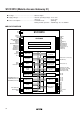
S1C33210 (Mobile Access Gateway IC)
■ PIN FUNCTION
● Pins for Power Supply System
Function
Power supply pin (+)
Power supply pin (-) GND
Analog system power supply (+); AVDD = VDD
Pull-up
–
–
–
I/O
–
–
–
Pin name
VDD x6
VSS x7
AVDD
Pin No.
8, 27, 47, 74, 93, 111
3, 22, 39, 54, 67, 90, 102
30
● Pins for Clock Generator
Function
Low-speed (OSC1) oscillation input
Low-speed (OSC1) oscillation output
High-speed (OSC3) oscillation input
High-speed (OSC3) oscillation output
PLL set-up pins
Capacitor connecting pin for PLL
Pull-up
–
–
–
–
–
–
I/O
I
O
I
O
I
–
Pin name
OSC1
OSC2
OSC3
OSC4
PLLS[1:0]
PLLC
Pin No.
51
50
112
113
105, 106
103
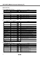
● Pins for External Bus Interface Signals
Function
Address bus (A0)/bus strobe (low byte) signal
Address bus (A1 to A23)
Data bus (D0 to D15)
Area 10 chip enable for external memory
Chip enable (area 9, 17)
Chip enable (area 8, 14)/DRAM row strobe (Area 8, 14)
Chip enable (area 7, 13)/DRAM row strobe (Area 7, 13)
Area 6 chip enable
Chip enable (area 5, 15)
Chip enable (area 4, 11)
Read signal
Write (low byte) signal/write signal/DRAM write signal
Write (high byte) signal/bus strobe (high byte) signal
DRAM column address strobe (high byte) signal
DRAM column address strobe (low byte) signal
Bus clock output
I/O port/Bus release request input/Area 6 chip enable
I/O port/Bus release request acknowledge output
I/O port/Wait cycle request input/Area 4 and 5 chip enable
I/O port/DRAM read signal output for successive RAS mode
I/O port/DRAM write signal output for successive RAS mode/
Area address strobeoutput for GA
I/O port/Bus status monitor signal output for bus release request/
Area read signal output GA
Area 10 boot mode selection
Pull-up
–
–
–
–
–
–
–
–
–
–
–
–
–
–
–
–
–
–
–
–
–
–
Pull-up
–
I/O
O
O
I/O
O
O
O
O
O
O
O
O
O
O
O
O
O
I/O
I/O
I/O
I/O
I/O
I/O
I
I
Pin name
A0/#BSL
A[23:1]
D[15:0]
#CE10EX/#CE9&10EX
#CE9/#CE17/#CE17&18
#CE8/#RAS1/#CE14/#RAS3
#CE7/#RAS0/#CE13/#RAS2
#CE6/#CE7&8
#CE5/#CE15/#CE15&16
#CE4/#CE11/#CE11&12
#RD
#WRL/#WR/#WE
#WRH/#BSH
#HCAS
#LCAS
BCLK
P34/#BUSREQ/#CE6
P35/#BUSACK
P30/#WAIT/#CE4&5
P20/#DRD
P21/#DWE/#GAAS
P31/#BUSGET/#GARD
EA10MD1
EA10MD0
Pin No.
55
56–58, 63–66, 69, 70, 72,
75, 78, 81, 84, 85, 87–89,
91, 73, 76, 79, 82
7, 10, 12, 14, 16, 18, 25,
26, 36–38, 40–42, 45, 46
34
48
53
49
52
71
35
24
20
21
60
61
4
62
59
68
92
117
11
115
114
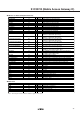
● HSDMA Control Signal Pins
Function
Input port/HSDMA Ch.0 request input
Input port/HSDMA Ch.1 request input
I/O port/HSDMA Ch.0 acknowledge output
I/O port/HSDMA Ch.1 acknowledge output
I/O port/Serial I/F Ch.1 data input/
HSDMA Ch.2 acknowledge output
I/O port/16-bit timer 4 event counter input/
HSDMA Ch. 0 end-of-transfer signal output
I/O port/16-bit timer 5 event counter input/
HSDMA Ch.1 end-of-transfer signal output
I/O port/Serial I/F Ch.1data output/
HSDMA Ch.2 end-of-transfer signal output
Pull-up
Pull-up
Pull-up
–
–
–
–
–
–
I/O
I
I
I/O
I/O
I/O
I/O
I/O
I/O
Pin name
K50/#DMAREQ0
K51/#DMAREQ1
P32/#DMAACK0
P33/#DMAACK1
P04/SIN1/#DMAACK2
P15/EXCL4/#DMAEND0
P16/EXCL5/#DMAEND1
P05/SOUT1/#DMAEND2
Pin No.
19
23
13
15
83
128
77
86