
Service manual


EPSON FX-890/2190 Revision B
Appendix Connector Summary 106
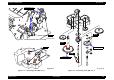
Parallel I/F (CN1)
Refer to “Parallel interface (Forward channel)” (page 23).
Type-B I/F (CN2)
Refer to “Type-B Interface communication specification” (page 27).
USB I/F (CN3)
Refer to “USB Interface” (page 26).
PG Detector (CN5)
Front PE Detector (CN6)
Rear PE Detector(CN7)
HP Detector(CN8)
Release Detector(CN11)
CR Motor (12)
PF Motor (CN13)
Table 7-2. Connector Pin Assignment - CN5
Pin No. I/O Signal Name Function
1 I PG1 PG Detector signal
2 - GND Ground
Table 7-3. Connector Pin Assignment - CN6
Pin No. I/O Signal Name Function
1 I PE Front PE Detector signal
2 - GND Ground
Table 7-4. Connector Pin Assignment - CN7
Pin No. I/O Signal Name Function
1- +5V+5V
2 I PE Rear PE Detector signal
3 - GND Ground
Table 7-5. Connector Pin Assignment - CN8
Pin No. I/O Signal Name Function
1 I HP HP Detector signal
2 - GND Ground
Table 7-6. Connector Pin Assignment - CN11
Pin No. I/O Signal Name Function
1 I RELEASE Release Detector signal
2 - GND Ground
Table 7-7. Connector Pin Assignment - CN12
Pin No. I/O Signal Name Function
1 O CRA CR Motor phase A
2 O CR-A CR Motor phase /A
3 O CRB CR Motor phase B
4 O CR-B CR Motor phase /B
5 - CRCOM Common
Table 7-8. Connector Pin Assignment - CN13
Pin No. I/O Signal Name Function
1 O PFA PF Motor phase A
2 O PFB PF Motor phase B
3 O PF-A PF Motor phase /A
4 O PF-B PF Motor phase /B