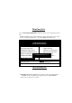
Read me first 1. The "LOAD SETUP DEFAULTS" function loads the system default data directly from ROM and initializes the associated hardware properly. This function is necessary when you accept this mainboard, or the system CMOS data will corrupt. ROM PCI/ISA BIOS CMOS SETUP UTILITY AWARD SOFTWARE, INC.
Apollo MVP3 AGPset EP-58MVP3C-M ISA/PCI/AGP MainBoard with Onboard PCI IDE and Super Multi-I/O. TRADEMARK All products and company names are trademarks or registered trademarks of their respective holders. The specification is subject to change without notice.
Package Checklist Please check your package which should include all items listed below. If you find any item damaged or missed, please contact your supplier.
Contents page Chapter 1 - Introduction....................................................... Chapter 2 - Hardware Design........................................... . 2-1 Mainboard Layout................................................................ 2-2 Connectors and Jumpers........................................................... 2-3 System Memory Configuration................................................ 2-4 ATX Power ON/OFF Control....................................................
Introduction 1-1 Chapter 1 Introduction This mainboard is a high performance system hardware based on Intel Pentium processor and is equipped with an AGP slot, four PCI slots, three standard ISA slots, Super Multi-I/O controller and dual port PCI-IDE connectors for the future expansion. The hardware dimension is 220mm x 260mm with a four-layer-design technology. Specification VIA Apollo MVP3 AGP/PCIset chipset.
Hardware Design 2-1 Chapter 2 Hardware design 2-1 Mainboard Layout This mainboard is designed with VIA Apollo MVP3 AGP/PCIset chipset which is developed by VIA Corporation to fully support Pentium Processor PCI/ ISA system. By providing a massive increase in the bandwidth available between the video card and the processor (66MHz), the unique feature of AGP supported by VIA Apollo MVP3 chipset improves the speed of rendering and texturing for 3D graphics.
2-2 EP-58MVP3C-M EP-58MVP3C-M Layout CN1 1 COM1 5 W83877TF 1 K/B CONN. J1 JP4 PRINTER FDD CONN. Primary IDE Secondary IDE J7 AT Power Conn. Conn. USB CONN. BIOS COM2 ATX Power DIMM2 Bank 0 Bank 1 DIMM3 DIMM1 EP- 58MVP3C- M AGP PCI#1 PCI#2 PCI#3 PCI#4 BIOS 82C586B 2.1V 2.2V 2.8V 2.9V 3.2V JP2 Bank 2 VT82C598AT 1 6 Socket 7 5 10 CACHE 1 J4 : CPU FAN J6 : CHASSIS FAN J4 J2 J3 1 5 RESET SPEAKER KEYLOCK Figure 2-1 1 5 IR CONN.
Hardware Design 2-3 2-2 Connectors and Jumpers This section describes the connectors and jumpers equipped in the mainboard. Please refer to Figure 2-1 for the location of each connector and jumper. JP3 1 2 Multiplier 2X 2.5 X 3X 3.5 X 4X 4.
2-4 EP-58MVP3C-M J2 Reset Switch - Closed to restart system. 1 4 1 5 J3 Speaker - connect to the system's speaker for beeping. 1. Speaker 2. N/C 3. GND 4. VCC KeyLock - Keyboard lock switch & Power LED connector. 1. Power LED(+) 2. N/C 3. GND 4. Key-Lock 5. GND 5 IrDA/ASK IR CONNECTOR 1. VCC 2. NC 3. IRRX 4. GND 5. IRTX + IDE LED indicator - LED ON when harddisks activate. + Turbo LED indicator - LED ON when higher speed is selected.
Hardware Design 2-5 2-3 System Memory Configuration This mainboard supports different type of settings for the system memory. The following figures and table provides all possible memory combinations. 12 12 12 12 12 12 12> 12> DIMM3 DIMM2 > DIMM1 DIMM 1 BANK 0 DIMM 2 BAMK 1 8MB 16MB 32MB 64MB 1 128MB 8MB 16MB 32MB 64MB 1 128MB x x DIMM 3 BANK 2 8MB 16MB 32MB 64MB 1 128MB BANK 2 BANK 1 BANK 0 TOTAL MEMORY MAX.
2-6 EP-58MVP3C-M 2-4 ATX Power ON/OFF Control This mainboard equips an ATX power connector which is a single 20-PIN input device for an ATX power supply (see Figure 2-2). An ATX power supply provides a build-in Remote Power ON/OFF function. To implement the function, a momentary switch which is normally open should be connected to the position J3(PIN 12, 13) as the system's power ON/OFF button. Note that an AT power supply does not offer this function.
Hardware Design 2-7 2-5 External Modem Ring-in Power ON and Keyboard Power ON Functions On the basis of bounded functions in I/O chipset, the two serial ports are able to support the External Modem Ring-in Power ON function. Once users connect the external modem to COM1 or COM2, this mainboard mainboard allows users to turn on their system through the remote and host's dial-up control.
2-8 EP-58MVP3C-M 2-6 Integrated PCI Bridge This mainboard utilizes VIA Apollo MVP3 AGP/PCIset chipset to support Intel Pentium Processor PCI/ISA system. The VIA Apollo MVP3 PCIset chipset consists of the 82C598AT system controller (TSC), and one 82C586B PCI ISA/ IDE Accelerator bridge chip. It provides an interface which translates CPU cycle into PCI bus cycle, and PCI burst read/write capability.
AWARD BIOS 3-1 CHAPTER 3 AWARD BIOS SETUP Award's ROM BIOS provides a built-in setup program which allows user to modify the basic system configurations and hardware parameters. The modified data will be stored in a battery-backed CMOS RAM so that data will be retained even when the power is turned off. In general, the information saved in the CMOS RAM stays unchanged unless there is a configuration change in the system, such as a hard drive replacement or a new device installation.
3-2 CHAPTER 3 3-1 STANDARD CMOS SETUP Choose "STANDARD CMOS SETUP" in the CMOS SETUP UTILITY Menu (Fig. 3-1). The STANDARD CMOS SETUP allows user to configure system setting such as the current date and time, type of hard disk installed, floppy type, and display type. Memory size is auto-detected by the BIOS and displayed for your reference.
AWARD BIOS 3-3 ROM PCI/ISA BIOS(2A5LEPA9) BIOS FEATURES SETUP AWARD SOFTWARE, INC.
3-4 CHAPTER 3 Quick Power On Self Test:This category speeds up Power On Self Test (POST) after you power on the computer. If it is set to Enable, BIOS will shorten or skip some checking items during POST. Enabled : Enable quick POST. Disabled: Normal POST. Boot Sequence:This category determines which drive is searched first for the O/S(Operating System).The default value is A,C. A,C :The system will search for floppy disk drive first then hard disk drive.
AWARD BIOS 3-5 Typematic Rate Setting: This determines the typematic rate. Enabled : Enable typematic rate and typematic delay programming. Disabled: Disable typematic rate and typematic delay programming. The system BIOS will use default value of 2 items and the default is controlled by the keyboard. Typematic Rate(Chars/Sec): 6 : 6 characters per second. 10: 10 characters per second. 15: 15 characters per second. 24: 24 characters per second. 8 : 8 characters per second. 12: 12 characters per second.
3-6 CHAPTER 3 C8000 CC000 D0000 D4000 D8000 DC000 - CBFFF CFFFF D3FFF D7FFF DBFFF DFFFF Shadow : Shadow: Shadow: Shadow: Shadow: Shadow: These categories determine whether optional ROM will be copied to RAM by 16K byte or 32K byte per unit and the size depends on the chipset. Enabled : Optional shadow is enabled. Disabled: Optional shadow is disabled. 3-3 CHIPSET FEATURES SETUP Choose the "CHIPSET FEATURES SETUP" in the CMOS SETUP UTILITY menu to display the following menu.
AWARD BIOS 3-7 DRAM Timing: The default value is 60ns. 60ns : 2 (faster) Burst Wait State, for 60~70ns Fast Page Mode/EDO DRAM. 70ns : 3 (slower) Burst Wait State, for 70ns Fast Page Mode/EDO DRAM. SDRAM Cycle length: The default value is 2. 2 : 2 HCLKS. 3: 3 HCLKS. SDRAM Bank Interleave: The default value is 2 Bank. Disabled : Normal Setting. 2 Bank/4 Bank: SDRAM 2 or 4 Bank Interleave. DRAM Read Pipeline: The default value is Enabled. Disabled : Normal Setting.
3-8 CHAPTER 3 AGP Aperture Size: The amount of the system memory that the AGP card is allowed to share. The options available are 4M, 8M, 16M, 32M, 64M, 128M, 256M. The default value is 64M. AGP Transfer Mode: The default value is 1X. 1X : 66MHz AGP transfer mode. 2X: 133MHz AGP transfer mode. Cyrix M2 ADS# Delay: The default value is Enabled. Disabled : Normal Setting. Enabled: Delay 1 HCLK for Cyrix 6x86MX when the ADS# assert. System/CPU Warning Temp: The default value is 66C/151F.
AWARD BIOS 3-9 3-4 POWER MANAGEMENT SETUP Choose the "POWER MANAGEMENT SETUP" in the CMOS SETUP UTILITY to display the following screen. This menu allows the user to modify the power management parameters and IRQ signals. In general, these parameters should not be changed unless it is absolutely necessary. ROM PCI/ISA BIOS(2A5LEPA9) POWER MANAGEMENT SETUP AWARD SOFTWARE, INC.
3-10 CHAPTER 3 B. Time-out parameters : HDD Standby HDD Standby timer can be set from 1 to 15 minute(s). System Doze The "System Doze" mode timer starts to count when there is no "PM events" occurred. The valid time-out setting is from 1 minute up to 1 hour. System Suspend This function works only when the Pentium Procssor is installed. The timer starts to count when "System Standby" mode timer is timed out and no "PM Events" occurred. Valid range is from 1 minute up to 1 hour.
AWARD BIOS 3-11 RTC Alarm Resume This option allows you to have the system turn on at a preset time each day or on a certain day. This option is only available when used an ATX power supply. Enabled : The system will turn on at the preset time. Disabled : Normal Setting Date(of month) This field is to set the date that the system will turn on. The default value is 0. 0 : Turn on the system on everyday at the preset time. 1-31 : Represets the date of the month that you need the system to turn on.
3-12 CHAPTER 3 PM Events: AWARD BIOS defines 7 PM Events in the power management mode (Doze & suspend). The user can initialize any PM Events to be "Enable" or "Disable". When the system detects all of the enabled events do not have any activity, it will start the system Doze timer first if the "Power Management" is not "Disabled". Once the system Doze timer is timed out, it will process doze power saving procedure by starting the system suspend timer.
AWARD BIOS 3-13 Resource Controlled By:The default value is Manual. Manual: The field defines that the PNP Card's resource is controlled by manual. You can setup whether IRQ-X or DMA-X is assigned to PCI/ISA PNP or Legacy ISA Cards. Auto: If your ISA card and PCI card are all PNP cards. Set this field to "Auto". The BIOS will assign the interrupt resource automatically. Reset Configuration Data: The default value is Disabled.
3-14 CHAPTER 3 3-6 INTEGRATED PERIPHERALS ROM PCI/ISA BIOS(2A5LEPA9) INTEGRATED PERIPHERALS WARD SOFTWARE, INC.
AWARD BIOS 3-15 IDE Primary Master PIO: The default value is Auto. Auto : BIOS will automatically detect the Onboard Primary Master PCI IDE HDD Accessing mode. Mode0~4 : Manually set the IDE Accessing mode. IDE Primary Slave PIO: The default value is Auto. Auto : BIOS will automatically detect the Onboard Primary Slave PCI IDE HDD Accessing mode. Mode0~4 : Manually set the IDE Accessing mode. IDE Secondary Master PIO: The default value is Auto.
3-16 CHAPTER 3 Onboard UART 2 Mode:The default value is standard. This field allows the User to select the COM2 port that can support a serial Infrared Interface. Standard: Support a Serial Infrared Interface IrDA. HPSIR: Support a HP Serial Infrared Interface format. ASKIR: Support a Sharp Serial Infrared Interface format. Onboard Parallel port: This field allows the user to sellect the LPT port. The default value is 378H/IRQ7.
AWARD BIOS 3-17 ROM PCI/ISA BIOS(2A5LEPA9) CMOS SETUP UTILITY AWARD SOFTWARE, INC.
3-18 CHAPTER 3 3-9 IDE HDD AUTO DETECTION The "IDE HDD AUTO DETECTION" utility is a very useful tool especially when you do not know which kind of hard disk type you are using. You can use this utility to detect the correct disk type installed in the system automatically. But now you can set HARD DISK TYPE to Auto in the STANDARD CMOS SETUP. You do not need the "IDE HDD AUTO DETECTION" utility. The BIOS will Auto-detect the hard disk size and model on display during POST.
AWARD BIOS 3-19 LBA (Logical Block Addressing) mode: This is a new HDD accessing method to overcome the 528 Megabyte bottleneck. The number of cylinders, heads and sectors shown in the setup may not be the number physically contained in the HDD. During the HDD accessing, the IDE controller will transform the logical address described by sector, head and cylinder into its own physical address inside the HDD. The maximum HDD size supported by LBA mode is 8.
3-20 CHAPTER 3 Note: To support LBA or LARGE mode of HDDs, there must be some softwares involved. All softwares are located in the Award HDD Service Routine (1NT 13h). It may fail to access a HDD with LBA (LARGE) mode selected if you are running under on Operating System which replaces the whole 1NT 13h. UNIX operating systems do not support either LBA or LARGE and must utilize the Standard mode. UNIX can support drives larger than 528MB.
TECHNICAL INFORMATION 4-1 Chapter 4 Technical Information 4-1 I/O & MEMORY MAP MEMORY MAP Address Range [00000-7FFFF] [80000-9FBFF] [9FC00-9FFFF] [A0000-C7FFF] [C8000-DFFFF] [E0000-EEFFF] [EF000-EFFFF] [F0000-F7FFF] [F8000-FCFFF] [FD000-FDFFF] [FE000-FFFFF] Size Description 512K Conventional memory 127K Extended Conventional memory 1K Extended BIOS data area if PS/2 mouse is installed 160K Available for Hi DOS memory 96K Available for Hi DOS memory and adapter ROMs 60K Available for UMB 4K Video service r
4-2 CHAPTER 4 4-2 TIME & DMA CHANNELS MAP TIME MAP: DMA CHANNELS : TIMER Channel 0 TIMER Channel 1 TIMER Channel 2 DMA Channel 0 DMA Channel 1 DMA Channel 2 DMA Channel 3 DMA Channel 4 DMA Channel 5 DMA Channel 6 DMA Channel 7 System timer interrupt. DRAM REFRESH request. SPEAKER tone generator. Available. Onboard ECP (Option). FLOPPY DISK (SMC CHIP). Onboard ECP (default). Cascade for DMA controller 1. Available. Available. Available. 4-3 INTERRUPT MAP NMI : IRQ (H/W) : Parity check error.
TECHNICAL INFORMATION 4-3 4-4 RTC & CMOS RAM MAP RTC & CMOS : 00 01 02 03 04 05 06 07 08 09 0A 0B 0C 0D 0E 0F 10 11 12 13 14 15 16 17 18 19-2d 2E-2F 30 31 32 33 34-3F 40-7F Seconds. Second alarm. Minutes. Minutes alarm. Hours. Hours alarm. Day of week. Day of month. Month. Year. Status register A. Status register B. Status register C. Status register D. Diagnostic status byte. Shutdown byte. FLOPPY DISK drive type byte. Reserve. HARD DISK type byte. Reserve. Equipment type. Base memory low byte.
4-4 CHAPTER 4 APPENDIX A: POST CODES ISA POST codes are typically output to port address 80h. POST(hex) DESCRIPTION 01-02 Reserved. C0 Turn off OEM specific cache, shadow. 03 1.Initialize EISA registers (EISA BIOS only). 2.Initialize all the standard devices with default values Standard devices includes. -DMA controller (8237). -Programmable Interrupt Controller (8259). -Programmable Interval Timer (8254). -RTC chip. 04 Reserved 05 1.Keyboard Controller Self-Test. 2.Enable Keyboard Interface.
TECHNICAL INFORMATION 4-5 POST(hex) DESCRIPTION 0C Initialization of the BIOS Data Area. (40:ON - 40:FF) 0D 1.Program some of the Chipset's value according to Setup. (Early Setup Value Program) 2.Measure CPU speed for display & decide the system clock speed. 3.Video initialization including Monochromc, CGA, EGA/VGA. If no display device found, the speaker will beep. 0E 1.Test video RAM. (If Monochromc display device found) 2.Show messages including.
4-6 CHAPTER 4 POST(hex) DESCRIPTION 32 1.Display the Award Plug & Play BIOS Extension message. (PnP BIOS only) 2.Program all onboard super I/O chips (if any) including COM ports, LPT ports, FDD port ... according to setup value. 33-3B Reserved. 3C Set flag to allow users to enter CMOS Setup Utility. 3D 1.Initialize Keyboard. 2.Install PS2 mouse. 3E Try to turn on Level 2 cache. Note : Some chipset may need to turn on the L2 cache in this stage. But usually, the cache is turn on later in POST 61h.
TECHNICAL INFORMATION 4-7 POST(hex) DESCRIPTION 52 1.Initialize all ISA ROMs. 2.Later PCI initializations. (PCI BIOS only) -assign IRQ to PCI devices. -initialize all PCI ROMs. 3.PnP Initialzations. (PnP BIOS only) -assign IO, Memory, IRQ & DMA to PnP ISA devices. -initialize all PnP ISA ROMs. 4.Program shadows RAM according to Setup settings. 5.Program parity according to Setup setting. 6.Power Management Initialization. -Enable/Disable global PM. -APM interface initialization. 53 1.
4-8 CHAPTER 4 APPENDIXB:I/OCONNECTORS J1 : PS/2 MOUSE CONNECTOR: 1 1. DATA 2. CLK 3. GND 4. NC 5. VCC CN1 : USB CONNECTOR: 1 8 9 16 Signal Name USB_VCC USB_data0USB_data0+ Ground USB_VCC USB_data1USB_data1+ Ground Pin Pin 1 2 3 4 5 6 7 8 Signal Name 9 10 11 12 13 14 25 26 Ground Ground Ground Ground Ground Ground Ground Ground COM1,COM2 : Serial Ports Connector Signal Name 1 6 5 10 DCD SIN SOUT DTR GND Pin Pin Signal Name 1 2 3 4 5 6 7 8 9 10 DSR RTS CTS RI N.C.
TECHNICAL INFORMATION 4-9 FDD1 : Floppy Disk Connector 1 33 2 34 Signal Name Pin Pin 1 3 5 7 9 11 13 15 17 19 21 23 25 27 29 31 33 2 4 6 8 10 12 14 16 18 20 22 24 26 28 30 32 34 Ground Ground Ground Ground Ground Ground Ground Ground Ground Ground Ground Ground Ground Ground Ground Ground Ground Signal Name FDHDIN Reserved FDEDIN IndexMotor Enable Drive Select BDrive Select AMotor Enable DIRSTEPWrite Data Write Gate Track 00Write ProtectRead DataSIDE 1 SELECTDiskette IDE1,IDE2 : Primary, Second
4-10 CHAPTER 4 Appendix C : AGP Driver for Windows 95 Installation Guide This section provides the information for installation of Apollo VP3 VxD Driver which supports Accelerated Graphics Port (AGP) functionalities. SYSTEM REQUIREMENTS 1.Microsoft Windows 95 OSR2.1 (OSR2.0 with USB upgrade) 2.VIA Apollo VP3 AGP Driver (Vgart.VXD) 3.AGP VGA Card with Driver 4.Direct X5 DDk or SDK INSTALLATION PROCEDURE Step 1. Install Windows 95 4.00.950 B or later version Step 2. Install USBSUPP (USB upgrade) Step 3.
TECHNICAL INFORMATION 4-11 b. Click on "Direct X" then c. Click on "Direct Draw" and d. Check if there are some values existing in the "Bit" and "overlays." if there is, that means the AGP can be activated properly. REPLACING AN EXISTING VGA CARD WITH THE AGP VGA CARD 1. Shut down the computer and then turn off the power 2. Replace the VGA card boot up the system once again 3. Now, Update Device Driver Wizard Window will appear.