
User`s manual


BIOS
Page 4-9
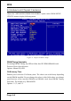
Active to Precharge Delay
This item specifies the number of clock cycles needed after a bank active command
before a precharge can occur (sets the minimum RAS pulse width.). The default is by
DRAM SPD.
Options: 5, 6, 7.
DRAM RAS# to CAS# Delay
This item sets the timing parameters for the system memory such as the CAS (Column
Address Strobe) and RAS (Row Address Strobe). The default is by DRAM SPD.
Options: 2, 3.
DRAM RAS# Precharge
This item refers to the number of cycles required to return data to its original
location to close the bank or the number of cycles required to page memory
before the next bank activate command can be issued. The default is by DRAM SPD.
Options: 2, 3.
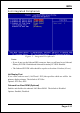
System BIOS Cacheable
This item allows the system to be cached in memory for faster execution. The
default is Enabled.
Options: Disabled, Enabled.
Video BIOS Cacheable
This item allows the video to be cached in memory for faster execution. The
default is Disabled.
Options: Disabled, Enabled.
Delayed Transaction
The mainboards chipset has an embedded 32-bit post write buffer to support delay
transactions cycles. Select Enabled to support compliance with PCI specification
version 2.1. The default is Enabled.
Options: Disabled, Enabled.
Command Per Clock
Enabling this item improves performance. The default is Auto.
Options: Auto, Enabled, Disabled.