
Specifications

Computer Architecture and Maintenance (G-Scheme-2014)
The new chips are expected to run at 1.2 V or less, versus the 1.5 V of DDR3 chips,
and have in excess of 2 billion data transfers per second. They are expected to be
introduced at frequency rates of 2133 MHz, estimated to rise to a potential 4266 MHz
and lowered voltage of 1.05 V by 2013.
DDR4 will not double the internal prefetch width again, but will use the same 8n
prefetch as DDR3. Thus, it will be necessary to interleave reads from several banks to
keep the data bus busy.
In February 2009, Samsung validated 40 nm DRAM chips, considered a "significant
step" towards DDR4 development since as of 2009, current DRAM chips were only
beginning to migrate to a 50 nm process. In January 2011, Samsung announced the
completion and release for testing of a 30 nm 2 GB DDR4 DRAM module. It has a
maximum bandwidth of 2.13 Gbit/s at 1.2 V, uses pseudo open drain technology and
draws 40% less power than an equivalent DDR3 module.
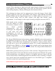
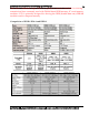
Feature of SDRAM , DDR and it versions0
Type Feature changes
SDRAM
Vcc = 3.3 V
Signal: LVTTL
DDR1
Access is ≥2 words
Double clocked
Vcc = 2.5 V
2.5 - 7.5 ns per cycle
Signal: SSTL_2 (2.5V)[18]
DDR2
Access is ≥4 words
"Burst terminate" removed
4 units used in parallel
1.25 - 5 ns per cycle
Internal operations are at 1/2 the clock rate.
Signal: SSTL_18 (1.8V)[18]
DDR3
Access is ≥8 words
Signal: SSTL_15 (1.5V)[18]
Much longer CAS latencies
DDR4 Vcc ≤ 1.2 V point-to-point (single module per channel)
Prepared By – Prof. Manoj.kavedia (9860174297 – 9324258878 ) (www.kavediasir.yolasite.com)
78