
Specifications

Computer Architecture and Maintenance (G-Scheme-2014)
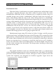
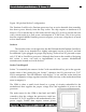
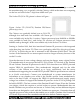
Socket 8
Socket 8 is a special SPGA socket featuring a whopping 387 pins! This was specifically
designed for the Pentium Pro processor with the integrated L2 cache. The additional
pins are required by the P6 processor bus. Figure. shows the Socket 8 pinout.
Figure. Socket 8 (Pentium Pro) pinout showing power pin locations.
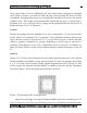
Socket 370 (PGA-370)
In November 1998, Intel introduced a new socket for P6 class processors. The socket
was called Socket 370 or PGA-370 because it has 370 pins and originally was designed
for lower-cost PGA versions of the Celeron and Pentium III processors. Socket 370 was
originally designed to directly compete in the lower-end system market along with the
Super7 platform supported by AMD and Cyrix. However, Intel later used it for the
Pentium III processor. Initially all the Celeron and Pentium III processors were made in
SECC or SEPP format. These are essentially circuit boards containing the processor and
separate L2 cache chips on a small board that plugs into the motherboard via Slot 1.
This type of design was necessary when the L2 cache chips were made a part of the
processor but were not directly integrated into the processor die. Intel did make a
multiple-die chip package for the Pentium Pro, but this proved to be a very expensive
way to package the chip, and a board with separate chips was cheaper, which is why
the Pentium II looks different from the Pentium Pro.
Starting with the Celeron 300A processor introduced in August 1998, Intel began
combining the L2 cache directly on the processor die; it was no longer in separate chips.
With the cache fully integrated into the die, there was no longer a need for a board-
mounted processor. Because it costs more to make a Slot 1 board or cartridge-type
Prepared By – Prof. Manoj.kavedia (9860174297 – 9324258878 ) (www.kavediasir.yolasite.com)
28