Computer Architecture and Maintenance (G-Scheme-2014) MOTHERBOARD 1 CHAPTER-1 & ITS COMPONENT SPECIFIC OBJECTIVES 1.1 CPU – Concept like address lines, data lines, internal registers. 1.2 Modes of operation of CPU – Real mode, IA-32 mode, IA-32 Virtual Real Mode. 1.3 Process Technologies, Dual Independent Bus Architecture, Hyper Threading Technologies & its requirement. 1.4 Processor socket & slots. 1.5 Chipset basic, chipset Architecture, North / South bridge & Hub Architecture. 1.
Computer Architecture and Maintenance (G-Scheme-2014) 2 Address Bus It is a group of wires or lines that are used to transfer the addresses of Memory or I/O devices. It is unidirectional. In Intel 8085 microprocessor, Address bus was of 16 bits. This means that Microprocessor 8085 can transfer maximum 16 bit address which means it can address 65,536 different memory locations. This bus is multiplexed with 8 bit data bus.
Computer Architecture and Maintenance (G-Scheme-2014) 3 or receive data. The data bus also works as address bus when multiplexed with lower order address bus. Data bus is 8 Bits long. The word length of a processor depends on data bus, thats why Intel 8085 is called 8 bit Microprocessor because it have an 8 bit data bus. To increase the amount of data being sent (called bandwidth) by increasing either the cycling time or the number of bits being sent at a time, or both.
Computer Architecture and Maintenance (G-Scheme-2014) 4 System bus It is a group of conductors. It is used to transfer information (electrical signal ) between two units. It consists of Data Bus, Address Bus and Control Bus. Functions of Buses The functions of buses can be summarized as below: 1. Data sharing - All types of buses found on a computer must be able to transfer data between the computer peripherals connected to it.
Computer Architecture and Maintenance (G-Scheme-2014) Many different types of registers are common between most microprocessor designs. These are: 5 Program Counter (PC) This register is used to hold the memory address of the next instruction that has to executed in a program. This is to ensure the CPU knows at all times where it has reached, that is able to resume following an execution at the correct point, and that the program is executed correctly.
Computer Architecture and Maintenance (G-Scheme-2014) 6 Other general purpose registers These registers have no specific purpose, but are generally used for the quick storage of pieces of data that are required later in the program execution. In the model used here these are assigned the names A and B, with suffixes of L and U indicating the lower and upper sections of the register respectively. Modes of Operation of CPU Q.List and Describe Modes of Operation of CPU Ans.
Computer Architecture and Maintenance (G-Scheme-2014) 7 bit instructions using 16-bit internal registers and could address only 1 MB of memory using 20 address lines. All original PC software was created to work with this chip and was designed around the 16-bit instruction set and 1 MB memory model. For example, DOS and all DOS software, Windows 1.x through 3.x, and all Windows 1.x through 3.x applications are written using 16-bit instructions.
Computer Architecture and Maintenance (G-Scheme-2014) 8 programs; it otherwise can use only the 16-bit instructions and access memory within the same 1 MB memory map of the original 8088. Therefore, if you have a system with a current 32-bit or 64-bit processor running Windows 3.x or DOS, you are effectively using only the first megabyte of memory, leaving all the other RAM largely unused! New OSs and applications that ran in the 32-bit protected mode of the modern processors were needed.
Computer Architecture and Maintenance (G-Scheme-2014) 9 It’s also important to note that some 16-bit (DOS and Windows 3.x) applications misbehave in a 32-bit environment, which means they do things that even virtual real mode does not support. Diagnostics software is a perfect example of this. Such software does not run properly in a real mode (virtual real) window under Windows.
Computer Architecture and Maintenance (G-Scheme-2014) 10 Processors with 64-bit extension technology can run in real (8086) mode, IA-32 mode, or IA-32e mode. IA-32 mode enables the processor to run in protected mode and virtual real mode. IA-32e mode allows the processor to run in 64-bit mode and compatibility mode, which means you can run both 64-bit and 32-bit applications simultaneously.
Computer Architecture and Maintenance (G-Scheme-2014) instructions; a BIOS update is also needed. Newer multicore processors with 64-bit support include these instructions as well.
Computer Architecture and Maintenance (G-Scheme-2014) 12 32-bit hardware to mainstream 32-bit computing took 16 years. The first 64-bit PC processor was released in 2003, and 64-bit computing really didn’t become mainstream until the release of Windows 7 in late 2009.
Computer Architecture and Maintenance (G-Scheme-2014) 13 Process technologies Q.List and explain different Process technologies Ans. 1. Dual Independent Bus Architecture 2. Hyper threading 3.MutliCore Dual Independent Bus – Architecture The Dual Independent Bus (DIB) architecture was first implemented in the sixthgeneration processors from Intel and AMD. DIB was created to improve processor bus bandwidth and performance.
Computer Architecture and Maintenance (G-Scheme-2014) boosting performance. Overall, DIB architecture offers up to three times the bandwidth performance over a single-bus architecture processor. 14 Fig. Advantages of DIB 1.Faster cache Access 2.Improves Band Width 3.Bot busses are accessed simultaneously hence through put is improved 4.Allow Multiple simultaneous cache request.
Computer Architecture and Maintenance (G-Scheme-2014) 15 With Hyper-Threading, a microprocessor's "core" processor can execute two (rather than one) concurrent streams (or thread s) of instructions sent by the operating system. Having two streams of execution units to work on allows more work to be done by the processor during each clock cycle . To the operating system, the HyperThreading microprocessor appears to be two separate processors.
Computer Architecture and Maintenance (G-Scheme-2014) 16 A processor with HT Technology enabled can fill otherwise-idle time with a second process for each core, improving multitasking and performance of multithreading single applications.
Computer Architecture and Maintenance (G-Scheme-2014) 17 appear as a quad-core processor to the OS. These processors combined 64-bit instruction capability with dual internal cores—essentially two processors in a single package. These chips were the start of the multicore revolution, which has continued by adding more cores along with additional extensions to the instruction set. Intel introduced the first quad-core processors in November 2006, called the Core 2 Extreme QX and Core 2 Quad.
Computer Architecture and Maintenance (G-Scheme-2014) The diagram below illustrates how a single-core processor (left) and a dual-core processor (right) handle multitasking: 18 It’s important to realize that multicore processors don’t improve single-task performance much. If you play non-multithreaded games on your PC, it’s likely that you would see little advantage in a multi-core or hyperthreaded CPU.
Computer Architecture and Maintenance (G-Scheme-2014) 19 Processor Slot and Sockets Q.Write short note on Processor Slot and Sockets. Ans. CPU Socket A CPU socket or CPU slot is a mechanical component(s) that provides mechanical and electrical connections between a microprocessor and a printed circuit board (PCB). This allows the CPU to be replaced without soldering. Common sockets have retention clips that apply a constant force, which must be overcome when a device is inserted.
Computer Architecture and Maintenance (G-Scheme-2014) 20 The original slot, or Slot 1 (pictured below), was first released by the Intel Corporation in 1997 as a successor to the Socket 8. Later, AMD released another slot processor known as the Slot A in 1999. Both slots look similar but are not compatible. Later, Intel released the slot 2, which was a bigger slot used with the later versions of the Pentium II processors.
Computer Architecture and Maintenance (G-Scheme-2014) Pentium and Pentium Pro processor sockets. 21 Zero Insertion Force When the Socket 1 specification was created, manufacturers realized that if users were going to upgrade processors, they had to make the process easier. The socket manufacturers found that 100 lbs. of insertion force is required to install a chip in a standard 169-pin screw Socket 1 motherboard.
Computer Architecture and Maintenance (G-Scheme-2014) 22 Figure Intel Socket 1 pinout. The original DX processor draws a maximum 0.9 amps of 5V power in 33MHz form (4.5 watts) and a maximum 1 amp in 50MHz form (5 watts). The DX2 processor, or OverDrive processor, draws a maximum 1.2 amps at 66MHz (6 watts). This minor increase in power requires only a passive heatsink consisting of aluminum fins that are glued to the processor with thermal transfer epoxy.
Computer Architecture and Maintenance (G-Scheme-2014) 23 Notice that although the chip for Socket 2 is called Pentium OverDrive, it is not a full-scale (64-bit) Pentium. Intel released the design of Socket 2 a little prematurely and found that the chip ran too hot for many systems. The company solved this problem by adding a special active heatsink to the Pentium OverDrive processor. This active heatsink is a combination of a standard heatsink and a built-in electric fan.
Computer Architecture and Maintenance (G-Scheme-2014) Figure. 237-pin Intel Socket 3 configuration. 24 Notice that Socket 3 has one additional pin and several others plugged in compared with Socket 2. Socket 3 provides for better keying, which prevents an end user from accidentally installing the processor in an improper orientation. However, one serious problem exists: This socket can't automatically determine the type of voltage that is provided to it.
Computer Architecture and Maintenance (G-Scheme-2014) 25 The 66MHz OverDrive processor that replaced it consumes a maximum 2.7 amps (13.5 watts), including about 1 watt to drive the fan. Even the original 60MHz Pentium processor consumes up to 2.91 amps at 5V (14.55 watts). It might seem strange that the replacement processor, which is twice as fast, consumes less power than the original, but this has to do with the manufacturing processes used for the original and OverDrive processors.
Computer Architecture and Maintenance (G-Scheme-2014) 26 Figure. 320-pin Intel Socket 5 configuration. The Pentium OverDrive for Pentium processors has an active heatsink (fan) assembly that draws power directly from the chip socket. The chip requires a maximum 4.33 amps of 3.3V to run the chip (14.289 watts) and 0.2 amp of 5V power to run the fan (one watt), which results in a total power consumption of 15.289 watts.
Computer Architecture and Maintenance (G-Scheme-2014) 27 supplies for different processors, the VRM converts the 3.3V or 5V to the proper voltage for the particular CPU you are using. Intel released different versions of the Pentium and Pentium-MMX processors that ran on 3.3V (called VR), 3.465V (called VRE), or 2.8V. Equivalent processors from AMD, Cyrix, and others used voltages from 3.3V to 1.8V.
Computer Architecture and Maintenance (G-Scheme-2014) 28 Socket 8 Socket 8 is a special SPGA socket featuring a whopping 387 pins! This was specifically designed for the Pentium Pro processor with the integrated L2 cache. The additional pins are required by the P6 processor bus. Figure. shows the Socket 8 pinout. Figure. Socket 8 (Pentium Pro) pinout showing power pin locations. Socket 370 (PGA-370) In November 1998, Intel introduced a new socket for P6 class processors.
Computer Architecture and Maintenance (G-Scheme-2014) 29 processor instead of a socketed type, Intel moved back to the socket design to reduce the manufacturing cost—especially with the Celeron, which at that time was competing on the low end with Socket 7 chips from AMD and Cyrix. The Socket 370 (PGA-370) pinout is shown in Figure .. Figure. Socket 370 (PGA-370) Pentium III/Celeron pinout (top view). The Celeron was gradually shifted over to PGA-370, although for a time both were available.
Computer Architecture and Maintenance (G-Scheme-2014) 30 Installing a Pentium III processor in the FC-PGA package into an older motherboard is unlikely to damage the motherboard. However, the processor itself could be damaged. Pentium III processors in the 0.18-micron process operate at either 1.60V or 1.65V, whereas the Intel Celeron processors operate at 2.00V. The motherboard could be damaged if the motherboard BIOS fails to recognize the voltage identification of the processor.
Computer Architecture and Maintenance (G-Scheme-2014) 31 The processor uses five voltage ID (VID) pins to signal the VRM built into the motherboard to deliver the correct voltage for the particular CPU you install. This makes the voltage selection completely automatic and foolproof. Most Pentium 4 processors for Socket 423 require 1.7V. A small triangular mark indicates the pin-1 corner for proper orientation of the chip.
Computer Architecture and Maintenance (G-Scheme-2014) 32 moved to incorporate L2 cache on-die, and the low-cost Duron was manufactured only in an on-die cache version, there was no longer a need for the expensive cartridge packaging the original Athlon processors used. Socket A has 462 pins and 11 plugs oriented in an SPGA form (see Figure).
Computer Architecture and Maintenance (G-Scheme-2014) Socket 603 33 Socket 603 is used with the Intel Xeon processor in DP (dual processor) and MP (multiple processor) configurations. These are typically used in motherboards designed for use in network file servers. Figure shows Socket 603. Figure 3.25 Socket 603 is used by the Intel Xeon processor. Socket 754 Socket 754 is used with the initial releases of the AMD Athlon 64 processors.
Computer Architecture and Maintenance (G-Scheme-2014) 34 Socket 940 is used with the Socket 940 version of the AMD Athlon 64 FX, as well as most AMD Opteron processors (see Figure). Motherboards using this socket support only registered DDR SDRAM modules in dual-channel mode. Because the pin arrangement is different, Socket 939 processors do not work in Socket 940, and vice versa. Figure. Socket 940. The cutout corner and triangle at the lower left indicate pin 1.
Computer Architecture and Maintenance (G-Scheme-2014) Socket M2 35 In the second quarter of 2006, AMD introduced processors that use a new socket, called Socket M2 (see Figure ). AMD intends for M2 to be the eventual replacement for the confusing array of Socket 754, Socket 939, and Socket 940 form factors it uses for the Athlon 64, Athlon 64 FX, Athlon 64 X2, Opteron, and Socket 754 AMD Sempron processors. Figure. Socket M2. The cutout corner at the lower left indicates pin 1.
Computer Architecture and Maintenance (G-Scheme-2014) Slot 1 (SC242) 36 Slot 1, also called SC242 (slot connector 242 pins), is used by the SEC design that is used with the cartridge-type Pentium II/III and Celeron processors (see Figure). Figure. Slot 1 connector dimensions and pin layout. Slot 2 (SC330) Slot 2, otherwise called SC330 (slot connector 330 pins), is used on highend motherboards that support the Pentium II Xeon and Pentium III Xeon processors. Figure. shows the Slot 2 connector. Figure.
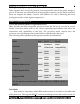
Computer Architecture and Maintenance (G-Scheme-2014) 37 Table 3.18. CPU Socket and Slot Types and Specifications Chip Class Socket Pins Layout Voltage Intel/AMD 486 class Socket 1 169 17x17 PGA 238 19x19 PGA Supported Processors Introduced 5V 486 SX/SX2, DX/DX2, Apr. '89 DX4 OD 5V 486 SX/SX2, DX/DX2, DX4 OD, 486 Mar. '92 Pentium OD 237 19x19 PGA 5V/3.3V 486 SX/SX2, DX/DX2, DX4, 486 Pentium Feb. '94 OD, AMD 5x86 Socket 6 [1] 235 19x19 PGA 3.
Computer Architecture and Maintenance (G-Scheme-2014) Chip Class Socket Pins Layout Voltage 38 Supported Processors Introduced D/Pentium Extreme Edition/LGA775 AMD class K7 Slot A 242 Slot Auto VRM AMD Athlon SECC 462 37x37 SPGA AMD Athlon/Athlon Auto VRM XP/Duron PGA/FC- June '00 PGA Socket 754 754 29x29 mPGA Auto VRM AMD Athlon 64 Sep. '03 Socket 939 939 31x31 mPGA Auto VRM AMD Athlon 64 v.2 June '04 Socket 940 940 31x31 mPGA Auto VRM Slot Auto VRM Pentium II/III Xeon Apr.
Computer Architecture and Maintenance (G-Scheme-2014) Chip Class Socket Pins Layout Voltage 39 Supported Processors Introduced PGA = Pin grid array PPGA = Plastic pin grid array SC242 = Slot connector, 242 pins SC330 = Slot connector, 330 pins SECC = Single edge contact cartridge SPGA = Staggered pin grid array mPGA = Micro pin grid array VRM = Voltage regulator module with variable voltage output determined by module type or manual jumpers Auto VRM = Voltage regulator module with automatic voltage s
Computer Architecture and Maintenance (G-Scheme-2014) The southbridge is slower than the northbridge, and information from the CPU has to go through the northbridge before reaching the southbridge. Other busses connect the southbridge to the PCI bus, the USB ports and the IDE or SATA hard disk connections. 40 Chipset selection and CPU selection go hand in hand, because manufacturers optimize chipsets to work with specific CPUs.
Computer Architecture and Maintenance (G-Scheme-2014) • • • 41 The IDE or ATA bus connects the southbridge to the disk drives. The AGP bus connects the video card to the memory and the CPU. The speed of the AGP bus is usually 66 MHz. The PCI bus connects PCI slots to the southbridge. On most systems, the speed of the PCI bus is 33 MHz. Also compatible with PCI is PCI Express, which is much faster than PCI but is still compatible with current software and operating systems.
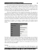
Computer Architecture and Maintenance (G-Scheme-2014) 42 Fig. Intel Hub Architecture (also called as AHA - Accelerated Hub Architecture) Intel introduced this hub architecture starting with the 820 chipset. The hub architecture divides control between a memory controller hub (MCH) that supports memory and AGP and an I/O controller hub (ICH) that supports PCI, USB, sound, IDE and LAN. The word hub in Intel Hub Architecture refers to the north and south bridges in a chipset.
Computer Architecture and Maintenance (G-Scheme-2014) 43 Fig. Because of the high-speed channel between the sections, the Intel Hub Architecture (IHA) is much faster than the earlier Northbridge/Southbridge design, which hooked all low-speed ports to the PCI bus. The IHA also optimizes data transfer based on data type.
Computer Architecture and Maintenance (G-Scheme-2014) 82810 Graphics Memory Controller Hub 44 The 82810 Graphics Memory Controller Hub (GMCH) is a MCH "north bridge" including a graphics controller and using Direct AGP (integrated AGP, where the graphics controller is directly connected to the system RAM) operating at 100 MHz. The 82810 chip features a "Hardware Motion Compensation" to improve soft DVD video and digital video out port for digital flat panel monitors.
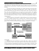
Computer Architecture and Maintenance (G-Scheme-2014) Q.State Function of North and South Bridge 45 Ans. South Bridge The southbridge is one of the two chips in the core logic chipset on a personal computer (PC) motherboard, the other being the northbridge. The southbridge typically implements the slower capabilities of the motherboard in a northbridge/southbridge chipset computer architecture. In Intel chipset systems, the southbridge is named Input/Output Controller Hub (ICH).
Computer Architecture and Maintenance (G-Scheme-2014) USB Port 7.1 Channel audio AC97 Modem Ehternet 46 drives. Hi-speed (JSB 2.0 ports. Option for integrated sound device with Dolby Digital and UTS. Integrated modem. Integrated 10/100 Mbs network controller. North Bridge The northbridge or host bridge was one of the two chips in the core logic chipset on a PC motherboard, used to managedata communications between a CPU and a motherboard.
Computer Architecture and Maintenance (G-Scheme-2014) 47 contrast to the other I/O devices, the AGP port is connected directly to the north bridge, because it has to be as close to the RAM as possible. The same goes for the PC Express x16 port, which is the replacement of AGP in new motherboards. Q.Why the name given North and South Bridge Ans. The name is derived from drawing the architecture in the fashion of a map.
Computer Architecture and Maintenance (G-Scheme-2014) 48 (among other factors) operating temperature; consequently most overclocking applications have software-imposed limits on the multiplier and external clock setting. Q.Describe the Chipset Architecture and State its Function Ans. The goals and needs of today’s computer hardware customer are more diverse than ever before. Some people have a need for speed.
Computer Architecture and Maintenance (G-Scheme-2014) 49 manufacturers. Intel and AMD provide specifications to the chipset manufacturers, who, in turn, develop and sell chipsets with various features and abilities to motherboard manufacturers. Of course, the exceptions to this are Intel and AMD, who also create their own chipsets.
Computer Architecture and Maintenance (G-Scheme-2014) the Southbridge chip. The Southbridge is the HUB that connects to slower I/O buses (for example, An ISA bus) to the system bus. 50 The Northbridge and the Southbridge are known as the chipset on the motherboard. These set of chips collectively control the memory cache, external bus, and some peripherals. There is a fast end of the hub, and there is a slow end of the hub.
Computer Architecture and Maintenance (G-Scheme-2014) can operate on both voltages, have two notches. Version 2.1 of the PCI standard introduced optional 66 Mhz operation. 51 A server-oriented variant of conventional PCI, called PCI-X (PCI Extended) operated at higher frequencies, up to 133 Mhz for PCI-X 1.0 and up to 533 Mhz for PCI-X 2.0. An internal connector for laptop cards, called Mini PCI, was introduced in version 2.2 of the PCI specification.
Computer Architecture and Maintenance (G-Scheme-2014) The signalling voltage does not equal the voltage of the motherboard power supply but rather the voltage threshold for the digital encryption of data. 52 There are 2 types of 32-bit connectors: • 32-bit PCI connector, 5V: • 32-bit PCI connector, 3.3V: The 64-bit PCI connectors offer additional pins and can accommodate 32-bit PCI cards. There are 2 types of 64-bit connectors: • 64-bit PCI connector, 5V: • 64-bit PCI connector, 3.3V: Q.
Computer Architecture and Maintenance (G-Scheme-2014) 53 Quatech's first data communication adapters were designed for the PC/ XT, and some of these are being used in older systems running extremely simple, low-speed applications. However, the ISA bus has come a long way since 1981, and its modern incarnation is much better suited to the PCs we use today and the applications we run on them. Features of ISA • They are two capabilities that handle data: 8-bit ISA and ISA-16 bits.
Computer Architecture and Maintenance (G-Scheme-2014) 54 a new video card and you are unsure about the slots, stick with the PCI version of this card it will always work. The most recent motherboards usually provide four or five PCI slots. The chipset provides bridging functions between these 10 buses (The PCI ISA bridge) and between 10 buses and other system buses, including the memory bus. Any system or motherboard today should provide PCI expansion slots in adequate number for s stem needs.
Computer Architecture and Maintenance (G-Scheme-2014) Parity on both data and address lines: This allows implementation of robust system. Support for both SV and 3.3 V operated logic. Forward and backward compatibility between 66 MHz and 33MHz PCI. 55 Q.List the specification and Version of PCI Ans. Versions of PCI allow (and in the latest versions require) 3.3V slots (keyed differently) on motherboards and allow for cards that are either double keyed for both voltages or even 3.3V only. • PC 2.
Computer Architecture and Maintenance (G-Scheme-2014) 32-bit or 64-bit bus width 32-bit address space (4 gigabytes) 32-bit I/0 port space (now deprecated) 256-byte configuration space 5-volt signaling Reflected-wave switching 56 Q.state basic difference between PCI , PCI-X and PCI-E Bus Ans. PCI-X uses a parallel interconnect along a bus that is shared with other PCI-X devices, just like PCI.
Computer Architecture and Maintenance (G-Scheme-2014) 57 PCI-Express, on the other hand, is brand-new, and is intended to replace AGP in the desktop market and ultimately be the de-facto high-bandwidth peripheral bus across all markets. Hardware that benefits from 64-bit PCI include: • High-performance graphics cards (PCI-Express only) in the 3D Gaming desktop and graphic intensive workstation markets. • U320 SCSI Controllers for high-speed hard disk access.
Computer Architecture and Maintenance (G-Scheme-2014) 58 Ans.PCI-X stands for PCI Extended. The PCI-X spec essentially doubled the bus width from 32 bits to 64 bits, thereby increasing bandwidth. The PCI's basic clock rate is increased to 66MHz with a 133MHz variety on the high end, providing another boost to the bandwidth and bringing it up to 1GB/s (at 133MHz).
Computer Architecture and Maintenance (G-Scheme-2014) A Bitflow R64 PCI-X frame grabber. Q.Is PCI-E any better? Ans.PCI-E stands fro PCI Express and is also known as 3GIO (Third Generation I/O) The most fundamental improvement is the adoption of point-to-point bus topology. In a point-to-point bus topology, a shared switch replaces the shared bus as the single shared resource by means of which all of the devices communicate.
Computer Architecture and Maintenance (G-Scheme-2014) 60 The connections between the devices and the switch is called a link and each link is consists of a number of lanes. Each lane is able to carry data in both directions. The gain in bandwidth is considerable as each lane can carry 2.5Gps in each direction. The PCI Express slot is available in versions of from 1 lane to 32 lanes and are called x1, x2, x4, x8, x16 and x32. The slot and connector are different lengths for each version. Q.
Computer Architecture and Maintenance (G-Scheme-2014) 61 Cache Memory Q.Write Short on Cache Memory Ans. cachememory is a high-speed memory buffer that temporarily stores data the processor needs, allowing the processor to retrieve that data faster than if it came from main memory. But there is one additional feature of a cache over a simple buffer, and that is intelligence. A buffer holds random data, usually on a first-in, first-out basis or a first-in, lastout basis.
Computer Architecture and Maintenance (G-Scheme-2014) 62 Disk caching applies the same principle to the hard disk that memory caching applies to the CPU. Frequently accessed hard disk data is stored in a separate segment of RAM in order to avoid having to retrieve it from the hard disk over and over. In this case, RAM is faster than the platter technology used in conventional hard disks. This situation will change, however, as hybrid hard disks become ubiquitous.
Computer Architecture and Maintenance (G-Scheme-2014) 63 Operation Let us suppose that the system has cache of three levels (level means that overall cache memory is split into different hardware segments which vary in their processing speed and memory). From RAM data is transferred into cache of 3 rd level (L3 cache). L3 cache is a segment of overall cache memory. L3 cacheis faster than RAM but slower then L2 cache. To further fasten up the process cache of second order L2 cache are used.
Computer Architecture and Maintenance (G-Scheme-2014) 64 When the processor needs to read from or write to a location in main memory, it first checks whether a copy of that data is in the cache. If so, the processor immediately reads from or writes to the cache, which is much faster than reading from or writing to main memory. The CPU uses cache memory to store instructions that are repeatedly required to run programs, improving overall system speed.
Computer Architecture and Maintenance (G-Scheme-2014) 65 not have louse the motherboard’s system bus for data transfer. Whenever data must be passed through the system bus, the data transfer speed s to the motherboard’s capability. The CPU can process data much faster by avoiding the bottleneck created by the system bus. As it happens, once most programs are open and running, they use very few resources. When these resources are kept in cache, programs can operate more quickly and efficiently.
Computer Architecture and Maintenance (G-Scheme-2014) 66 L2 cache was first introduced with the Intel Pentium and Pentium Pro computers and has been included with ever process since, with the exception of the early versions of Celeron processor. This cache is not as fast as the L1 cache, but is only slightly slower since it is still located on the same processor chip, and is still faster than the computers memory. The L2 cache is the second thing the computer looks at when performing instructions. L2,.
Computer Architecture and Maintenance (G-Scheme-2014) 67 • The same block of data which are stored on the main memory resides on the cache. Thus the instructions takes less time to execute. • The CPU and the cache are connected with a local bus which is of high capacity and speed due to which the data transfer is quick. • Cache memory is intelligent memory. • It holds current working set of code and data. • It reduces wait state or no wait states (LI cache) in system.
Computer Architecture and Maintenance (G-Scheme-2014) 68 Note : Multi-core processors include separate L1 caches for each processor core. Also, L1 cache is divided into equal amounts for instructions and data. To understand the importance of cache, you need to know the relative speeds of processors and memory.
Computer Architecture and Maintenance (G-Scheme-2014) 69 that the cache has the correct data 90% of the time, and consequently the processor runs at full speed (233 MHz in this example) 90% of the time. However, 10% of the time the cache controller guesses incorrectly, and the data has to be retrieved out of the significantly slower main memory, meaning the processor has to wait. This essentially throttles the system back to RAM speed, which in this example was 60 ns or 16 MHz.
Computer Architecture and Maintenance (G-Scheme-2014) 70 faster multicore processors such as the Intel Core i7 and AMD Phenom II and FX processors. L3 cache proves especially useful in multicore processors, where the L3 is generally shared among all the cores. Both Intel and AMD use L3 cache in most of their current processors because of the benefits to multicore designs.
Computer Architecture and Maintenance (G-Scheme-2014) 71 and at RAM speed about 1% (10% of 10%) of the time (16 MHz in this case). You can clearly see the importance of both the L1 and L2 caches; without them the system uses main memory more often, which is significantly slower than the processor. Important Point to be noted.
Computer Architecture and Maintenance (G-Scheme-2014) 72 OverView and Features of SDRAM , DDR, DDR2 and DDR3 Q.What is SDRAM Ans. Synchronous dynamic random access memory (SDRAM) is dynamic random access memory (DRAM) with an interface synchronous with the system bus carrying data between the CPU and the memory controller hub. SDRAM has a rapidly responding synchronous interface, which is in sync with the system bus. SDRAM waits for the clock signal before it responds to control inputs.
Computer Architecture and Maintenance (G-Scheme-2014) 73 because of the extra logic features. But the benefits of SDRAM allowed more than one set of memory, which increased the bandwidth efficiency. With the introduction of DDR, SDRAM quickly began to fade out of use because DDR was cheaper and more cost effective. The SDRAM used a 168-pin while the DDR module used a 184-pin. SDRAM modules used a voltage of 3.3V and DDR used 2.6V, producing less heat.
Computer Architecture and Maintenance (G-Scheme-2014) 74 clock signal changes twice per transfer, while the data lines change at most once per transfer. When operating at a high bandwidth, signal integrity limitations constrain the clock frequency. By using both edges of the clock, the data signals operate with the same limiting frequency, thereby doubling the data transmission rate.
Computer Architecture and Maintenance (G-Scheme-2014) This type of SDRAM is slower than the DDR variants, because only one word of data is transmitted per clock cycle (single data rate). But this type is also faster than its predecessors EDO-RAM and FPM-RAM which took typically 2 or 3 clocks to transfer one word of data.
Computer Architecture and Maintenance (G-Scheme-2014) 76 DDR2 SDRAM DDR2 SDRAM is very similar to DDR SDRAM, but doubles the minimum read or write unit again, to 4 consecutive words. The bus protocol was also simplified to allow higher performance operation. (In particular, the "burst terminate" command is deleted.) This allows the bus rate of the SDRAM to be doubled without increasing the clock rate of internal RAM operations; instead, internal operations are performed in units 4 times as wide as SDRAM.
Computer Architecture and Maintenance (G-Scheme-2014) DDR3 SDRAM 77 DDR3 continues the trend, doubling the minimum read or write unit to 8 consecutive words. This allows another doubling of bandwidth and external bus rate without having to change the clock rate of internal operations, just the width. To maintain 800– 1600 M transfers/s (both edges of a 400–800 MHz clock), the internal RAM array has to perform 100–200 M fetches per second. Again, with every doubling, the downside is the increased latency.
Computer Architecture and Maintenance (G-Scheme-2014) 78 The new chips are expected to run at 1.2 V or less, versus the 1.5 V of DDR3 chips, and have in excess of 2 billion data transfers per second. They are expected to be introduced at frequency rates of 2133 MHz, estimated to rise to a potential 4266 MHz and lowered voltage of 1.05 V by 2013. DDR4 will not double the internal prefetch width again, but will use the same 8n prefetch as DDR3.
Computer Architecture and Maintenance (G-Scheme-2014) 79 Stub Series Terminated Logic (SSTL) is a group of electrical standards for driving transmission lines commonly used with DRAM based DDR memory IC's and memory modules. SSTL is primarily designed for driving the DDR (double-data-rate) SDRAM modules used in computer memory Comparision of DDR-1 DDr-2 and DDR-3 Prepared By – Prof. Manoj.kavedia (9860174297 – 9324258878 ) (www.kavediasir.yolasite.
Computer Architecture and Maintenance (G-Scheme-2014) 80 ODT : On-die termination (ODT) is the technology where the termination resistor for impedance matching in transmission lines is located inside a semiconductor chip instead of on a printed circuit board.
Computer Architecture and Maintenance (G-Scheme-2014) • • • • 81 in-line memory module (RIMM), which is similar in size and pin configuration to a standard DIMM. What makes RDRAM so different is its use of a special high-speed data bus called the Rambus channel. RDRAM memory chips work in parallel to achieve a data rate of 800 MHz, or 1,600 MBps. Since they operate at such high speeds, they generate much more heat than other types of chips.
Computer Architecture and Maintenance (G-Scheme-2014) 1) 2) 3) 4) 5) 6) 7) 8) Conventional memory Upper memory area High memory area Extended memory Expanded memory Video & RAM area Adapter and special purpose ROM Motherboard BIOS ROM. 82 Conventional or Base 32M memory: The original PC- 1 6 M /4 G XT type system was designed to use 1MB of EX T EN D E D M e mo r y memory space in RAM.
Computer Architecture and Maintenance (G-Scheme-2014) 83 Extended memory : Extended memory is above 1MB. This memory is usually not available to computer directly. It can be accessed through special software or program or driver, this memory is available in AT machines, not in XTs. The limit of extended memory is 16MB for 286 processor and for 386, 486 and higher processor the extended memory is up to 4GB. System based on new Pentiums have a limit of 64G of memory.
Computer Architecture and Maintenance (G-Scheme-2014) 84 developed by AST, Quadram and Ashton-Tate is known as EEMS (Extended EMS). EEMS enables programs to use extra memory for code as well as for data. The most recent version of EMS (created in 1987) is known as EMS 4.0 or LIM 4.0, LIM being the initials of the three companies that developed the specification: Lotus, Intel, and Microsoft. EMS 4.0 raises the available amount of memory to 32MB. Expanded memory relies on technical trick known as paging.
Computer Architecture and Maintenance (G-Scheme-2014) Disk caches 85 A disk cache is a program to speed up disk access by storing the most frequently use information in the computer's memory and reading ahead from the disk in anticipation. With floppy disks, the time saved can be spectacular. Writes are almost always performed to the disk to prevent loss of data in case of power failure. Example: PC-CACHE, as supplied with PC-Tools. A shareware product is EMMCACHE.
Computer Architecture and Maintenance (G-Scheme-2014) 86 It is sometimes up to 64K of real addresses but this is just a small portion of the whole expanded memory, which can be very large. The expanded memory requires hardware and/or software that maps the expanded memory to a piece of address space, in what is called a "page frame". Extended memory can be used as expanded memory by using software and the 80286 or 80386 chips to "remap" it to the lower 1MB.
Computer Architecture and Maintenance (G-Scheme-2014) • BIOS or CMOS Setup - Configuration program that allows you to configure hardware settings including system settings such as computer passwords, time, and date. 87 The BIOS provides those instructions.
Computer Architecture and Maintenance (G-Scheme-2014) 88 Q.How It Is Stored on a Computer • Traditional BIOS firmware is included on a computer motherboard as Read Only Memory (ROM). This means that the system is accessible but is not dynamically written to the way that a computer's hard drive is during operation. A battery on the motherboard keeps the data on it intact, even when the computer is turned off while not in use.
Computer Architecture and Maintenance (G-Scheme-2014) • • • • • • • 89 the type and placement of ports and connectors. Generally, you should choose the case to fit the mobo, not vice-versa. But if there is a case that you simply mustuse (either because it's the one you happen to have or because you really, really like that case), then make sure the motherboard you choose is of a compatible form factor. Processor support.
Computer Architecture and Maintenance (G-Scheme-2014) • • 90 first check the with the motherboard manufacturer to see if it is compatible, and then search the hardware newsgroups for the OS you will be using to see how that particular board has worked out for others. On-Board Features.
Computer Architecture and Maintenance (G-Scheme-2014) Manufacturer Socket 91 Used For Intel Socket 2011Intel’s most recent LGA socket. Used mostly by gamers for six core i7 processors. Intel Socket 1366Workstation class computer using the i7 core or the Xenon 3XXX series. Has the pins on the motherboard. Intel Socket 1156The average consumer socket for i3, i5, and i7 processors. Intel Socket 1155A newer version of the socket 1156.
Computer Architecture and Maintenance (G-Scheme-2014) 92 Not all motherboards are the same physical size. The most common size is ATX; however, the specification which created the ATX standard also provided for several alternate configurations. All ATX motherboards will have the same general configuration, with the major components located in the same places. While it is usually possible to mount a smaller motherboard into a computer case, mounting a larger one may be impossible.
Computer Architecture and Maintenance (G-Scheme-2014) 93 These dimensions are given only to help identify the type of motherboard currently in a computer. These motherboard standards not only affect the size of the motherboard, but also the configuration of the various connectors. Attempting to put an ITX motherboard into a computer case which previously housed an ATX motherboard can cause serious problems, as the card slots and connectors will not line up properly.
Computer Architecture and Maintenance (G-Scheme-2014) 94 Input-Output (I/O) Connectors Back in the early days of personal computers, most input and output functions were performed by expansion cards. Today’s motherboards bring all of those functions onboard, eliminating the need for buying and installing additional cards. The number and types of connectors available can be critically important to some users and some applications.
Computer Architecture and Maintenance (G-Scheme-2014) monitors, or to gain speed, a separate video card is still recommended. Graphics accelerator cards are especially useful for gaming. 95 SLI and Crossfire Compatibility This is of special importance to high-end gamers or others who are using 3D graphics. SLI and Crossfire are the methods for using multiple video cards together to increase performance and quality.
Computer Architecture and Maintenance (G-Scheme-2014) 96 done by adding eight extra 8-bit buses which allow the graphics controller to issue new AGP requests and commands at the same time with other AGP data flowing via the main 32 address/data (AD) lines. This results in improved overall AGP data throughput.
Computer Architecture and Maintenance (G-Scheme-2014) 97 Generally the CPU can more quickly access main memory than it can graphics local memory via AGP, and certainly faster than via the PCI bus. Q. What is the difference between an AGP and a PCI graphics card? Answer: The biggest difference between AGP and PCI graphics cards is that AGP cards can access the system memory to help with complex operations such as texture mapping. PCI cards can only access the memory available on the actual card.
Computer Architecture and Maintenance (G-Scheme-2014) • 1 AGP doesn't share bandwidth with other devices, whereas the PCI bus does share bandwidth. AGP PCI Pipelined Requests Non-pipelined 2 3 Address/Data de-multiplexed Peak at 533 MB/s in32 bits 4 Single target, single master Multi target, multi master Memory read/write only Link to entire system No other input/output operations High/low priority queues No priority queues 5 6 98 Address/Data multiplexed Peak at 133 MB/s in 32 bits Q.
Computer Architecture and Maintenance (G-Scheme-2014) 99 AGP's is pipelined therefore requests are executed in parallel, making execution faster than the non-pipelined PCI bus. • AGP's address/data is de-muxed, therefore the AGP pipeline can work with the data gotten from the de-mux. The PCI bus's address/data remained muxed so that the non-pipelined PCI bus works with the data gotten from the mux.
Computer Architecture and Maintenance (G-Scheme-2014) Latest Chipset for Motherboard CMOS Setup Prepared By – Prof. Manoj.kavedia (9860174297 – 9324258878 ) (www.kavediasir.yolasite.
Computer Architecture and Maintenance (G-Scheme-2014) 101 Additional - Information Q.State Feature of XT mother Board Ans.
Computer Architecture and Maintenance (G-Scheme-2014) • Wait states: • System board 1 • Adapter 1 Standard Feature • ROM size 40KB or 64KB • ROM shadowing No • Optional math coprocessor 8087 • Coprocessor speed 4.
Computer Architecture and Maintenance (G-Scheme-2014) ■ 20MB or 30MB hard disk drive (enhanced models) ■ Serial/parallel interface (enhanced models) ■ CMOS clock-calendar and configuration with battery backup ■ Keylock ■ 84-key keyboard or 101-key Enhanced keyboard (standard on newer models) ■ Switchable worldwide power supply 103 System Architecture • Microprocessor 80286 • Clock speed 6MHz or 8MHz • Bus type ISA (Industry Standard Architecture) • Bus width 16-bit • Interrupt levels 16 (11 usable) • Typ
Computer Architecture and Maintenance (G-Scheme-2014) Coprocessor speed 4 or 5.
Computer Architecture and Maintenance (G-Scheme-2014) Table . Differences Between PC/XT and AT Systems System Attributes PC/XT Type 8-Bit 16-, 32-, 64-Bit AT Type DMA channels 4 (3 usable) 8 (7 usable) Maximum RAM 1MB 16MB/4GB[1] or more Floppy controller speed 250Kbps 250, 300, 500, and 1000Kbps Standard boot drive 360KB 720KB or 1.2M, 1.44MB, and 2.
Computer Architecture and Maintenance (G-Scheme-2014) Storage Devices & Interfacing. Objective � To understand the Recording techniques in storage devices. � To understand the working of storage devices. 2.1 Recording Techniques: FM, MFM , RLL, perpendicular recording 2.2 Hard Disk construction and working. 2.3 Terms related to Hard Disk. Track, sector, cylinder, cluster, landing zone, MBR, zone recording, write pre-compensation. 2.4 Formatting: Low level, High level & partitioning. 2.
Computer Architecture and Maintenance (G-Scheme-2014) Display Devices & Interfacing Objective � To understand the construction and working of display devices like CRT, LCD. � To understand the Interfacing of above devices to PC. 3.1 CRT: - Block diagram & working of monochrome & colour Monitor 3.2 Characteristics of CRT Monitor :DOT Pitch, Resolution, Horizontal Scanning frequency, Vertical scanning frequency, Interlaced Scanning, Non-Interfaced scanning, Aspect ratio. 3.