
Datasheet
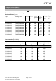

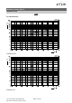


Dimensional drawing
Dimensions in mm
Case size
EIA / mm
l w h k
0201 / 0603 0.6 ±0.03 0.30 ±0.03 0.33 max. 0.15 ±0.05
0402 / 1005 1.0 ±0.15 0.50 ±0.10 0.6 max. 0.10 ... 0.30
0603 / 1608 1.6 ±0.15 0.80 ±0.10 0.9 max. 0.10 ... 0.40
0805 / 2012 2.0 ±0.20 1.25 ±0.15 1.4 max. 0.13 ... 0.75
1206 / 3216 3.2 ±0.30 1.60 ±0.20 1.7 max. 0.25 ... 0.75
1210 / 3225 3.2 ±0.30 2.50 ±0.25 1.7 max. 0.25 ... 0.75
1812 / 4532 4.5 ±0.40 3.20 ±0.30 2.5 max. 0.25 ... 1.00
2220 / 5750 5.7 ±0.40 5.00 ±0.40 2.5 max. 0.25 ... 1.00
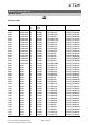
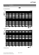
Recommended solder pad layout
Dimensions in mm
Case size
EIA / mm
A B C
0201 / 0603 0.30 0.25 0.30
0402 / 1005 0.60 0.60 0.50
0603 / 1608 1.00 1.00 1.00
0805 / 2012 1.40 1.20 1.00
1206 / 3216 1.80 1.20 2.10
1210 / 3225 2.80 1.20 2.10
1812 / 4532 3.60 1.50 3.00
2220 / 5750 5.50 1.50 4.20
Multilayer varistors (MLVs)
Standard series
Page 11 of 81Please read Cautions and warnings and
Important notes at the end of this document.