
User's Manual


USER MANUAL
PTM 215B – 2.4 GHZ Pusbutton Transmitter Module
© 2016 EnOcean | www.enocean.com F-710-017, V1.0 PTM 215B User Manual | v0.8 | September 2016 | Page 25/42
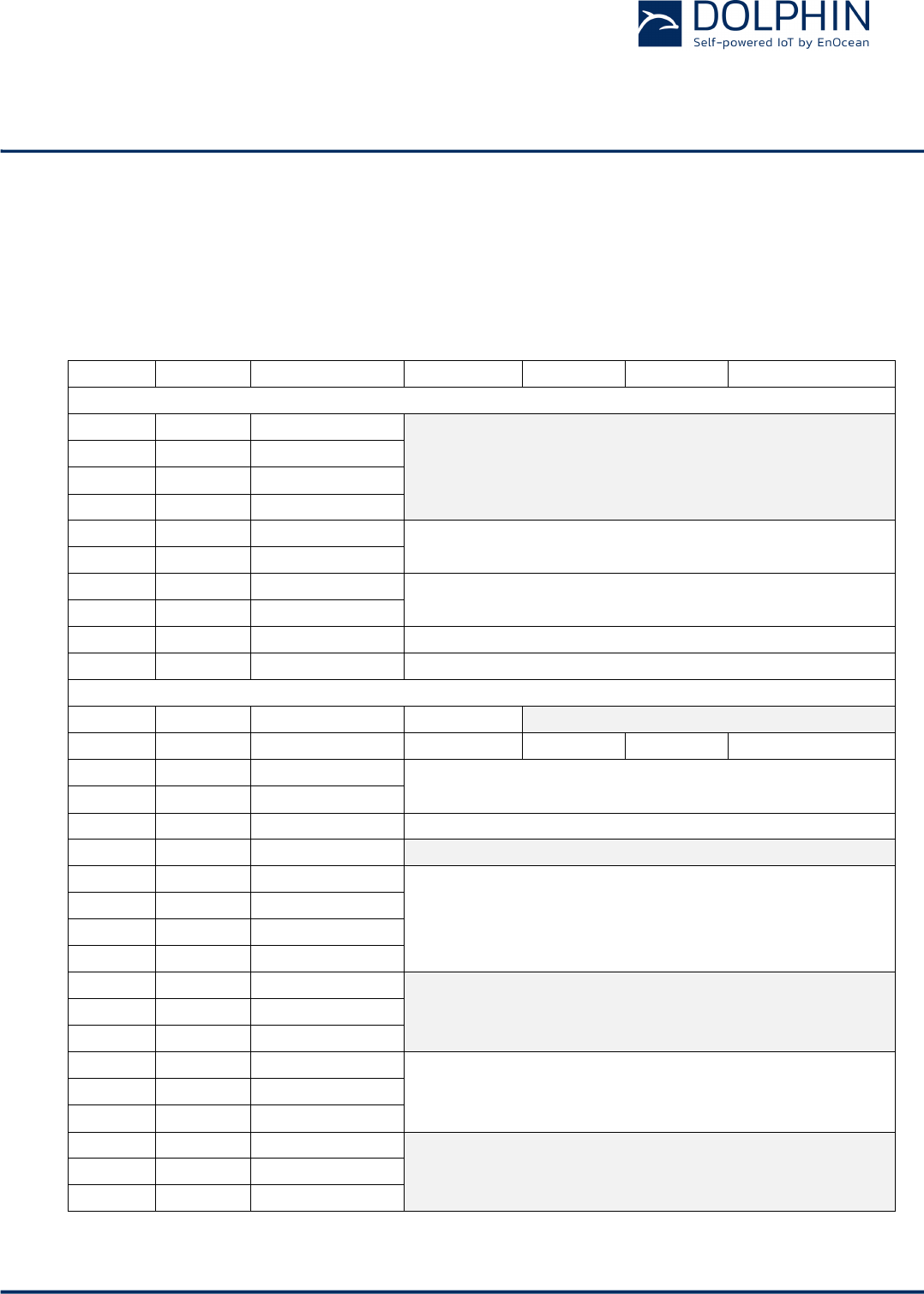
2.11.2 Memory Address Map
The NFC-accessible configuration memory is organized in memory pages where each
memory page is 4 byte wide. Each NFC access reads or writes one memory page.
The addresses map of the configuration memory is shown in Figure 19 below. The byte or-
der is little endian, i.e. Byte 0 will be read first and Byte 3 last.
Area
NFC Page
Total Byte Offset
Byte 0 (LSB)
Byte 1
Byte 2
Byte 3 (MSB)
Public Memory Area
Public
0x00
0
Reserved
Public
0x01
4
Public
0x02
8
Public
0x03
12
Public
0x04
16
Product Name "PTM 215B"
Public
0x05
20
Public
0x06
24
Product ID
Public
0x07
28
Public
0x08
32
Static Source Address
Public
0x09
36
Sequence Counter
Protected Memory Area
Protected
0x0A
40
Configuration
Reserved
Protected
0x0B
44
Opt Data 0
Opt Data 1
Opt Data 2
Opt Data 3
Protected
0x0C
48
Product ID Write
Protected
0x0D
52
Protected
0x0E
56
Source ID Write
Protected
0x0F
60
Reserved
Protected
0x10
64
Security Key Write
Protected
0x11
68
Protected
0x12
72
Protected
0x13
76
Protected
0x14
80
Reserved
Protected
…
…
Protected
0x1F
124
Protected
0x20
128
Custom NFC Data
Protected
…
…
Protected
0x5F
380
Protected
0x60
384
Reserved
Protected
…
…
Protected
0xE1
900
Figure 19 – Configuration memory address map