
- DBP SERIES USER MANUAL


54
DBP - Rev 6/93
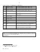
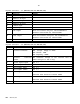
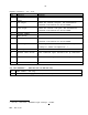
Signals connector - J1 (MBA-DBP/3UE and MBA-DBP/6UE)
Pin Function
Remarks
1 Channel A input
2 Channel -A input
3 Channel B input
4 Channel -B input
5 -Index input
6 Index input
7 +5V output
There are several +5V pins. The accumulative
external load should not exceed 200mA.
8 +15V output
There are several +15V pins. The accumulative
external load should not exceed 100mA.
9 Circuit common
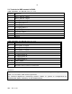
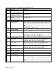
Signals connector - J2 (MBA-DBP/3UE and MBA-DBP/6UE)
Pin Function
Remarks
1 Resolver reference
Max. voltage: 20Vptp or 7Vrms
Max current: 80mA
Max frequency: 20KHz
2 Resolver reference
common.
The reference voltage to the resolver must be
taken from pins 1 and 2 only.
3 Cosine signal input.
See 7.3
4 Cosine signal common.
See 7.3
5 Sine signal input.
See 7.3
6 Sine signal common
See 7.3
7 +15V output
There are several +15V pins. The accumulative
external load should not exceed 100mA.
8 -15V output
There are several -15V pins. The accumulative
external load should not exceed 100mA.
9 Circuit common