0 Rev 6/93 DBP - Rev 6/93
1 ELMO-WARRANTY PERFORMANCE The warranty performance covers only ELMO's products and only the elimination of problems that are due to manufacturing defects resulting in impaired function, deficient workmanship or defective material. Specifically excluded from warranty is the elimination of problems which are caused by abuse, damage, neglect, overloading, wrong operation, unauthorized manipulations etc.
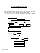
2 How to use this manual - Flow Chart The DBP HARDWARE MANUAL will lead you toward a successful start-up of your digital amplifier. Please review carefully the following flow chart and write down the chapters that you have to follow in the right order. Only after performing all the steps you may proceed to the software manual. If you are a new user of the DBP, you better not skip chapters 1-4 which will familiarize you with the product.
3 TABLE OF CONTENTS 1.Description ................................ .......................... 7 2. Type Designation ................................ ................... 8 3. Technical Specification ................................ ............ 9 3.1 Digital I/O specification ................................ ... 10 3.2 Analog input specification ................................ .. 13 3.3 Sensors specification ................................ ....... 14 3.4 4. 3.3.1 Encoder ......................
4 6. 7. Installation procedures ................................ ............ 65 6.1 Mounting................................ ..................... 65 6.2 Wiring................................ ....................... 65 6.3 Load inductance ................................ .............. 66 6.4 AC power supply ................................ .............. 66 6.5 Wiring diagrams ................................ .............. 67 Motor's windings ................................ .....67 6.5.
5 Appendix B - Adding a velocity feedback ............................... 101 Appendix C - Differential amplifier connection ........................ 102 DIMENSIONAL DRAWINGS ................................ ................... 103 PANEL (H), DBP1 ................................ .................. 104 PANEL (H), DBP2 ................................ .................. 107 PANEL (H), DBP3 ................................ .................. 110 PANEL (H), DBP4 ................................ ..........
6 1.Description The DBP series are digital, full wave, three phase servo amplifiers designed for high performance brushless servo motors in the range of up to 7KW. They utilize power MOSFETs and Surface Mounting Technology which contribute to its high efficiency and compact design. The DBP operates from a single AC supply (either single or three phase) and, when using the galvanic isolation option, it can be connected directly to the Mains.
7 * Standard commutation sensors: Hall effect sensors or a Resolver. * Galvanic isolation of the control stage - option. Digital Section Standard Features * Accepts motion commands via RS232 or RS485 * Buffering for pipe lining instructions prior to execution * Battery-backed RAM for storing user programs and parameters * Conditional statements for controlling program execution real- time.
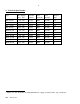
8 3. Technical Specification Type AC Supply * Current Size Size Weight min limits Panel(H) Rack(R) (Kg) max DBP-12/135 28- 135 12/24 DBP2 3U/20T 1.4 DBP-20/135 28- 135 20/40 DBP3 6U/21T 3 DBP- 8/270 100- 270 8/16 DBP2 3U/20T 1.4 DBP-16/270 100- 270 16/32 DBP3 6U/21T 3 DBPF-12/135 28- 135 12/24 DBP1 3U/13T 0.7 DBPF-20/135 28- 135 20/40 DBP4 6U/13T 1.3 DBPF-30/135 28- 135 30/60 DBP6 6U/21T 3 DBPF- 8/270 100- 270 8/16 DBP1 3U/13T 0.
9 General * DC output voltage is 130% of AC input voltage. * 2KHz current loop response * Outputs voltages of +5V/0.2A, +15V/0.1A for external use. * Efficiency at rated current - 97%. * Operating temperature: 0 - 50 °C. * Storage temperature: -10 - +70 °C. 3.1 Digital I/O specification Digital Inputs: High/Low input definition: Vil<1V, Vih>2.4V Maximum input voltage: 30V Input impedance: 3-7Kohm Input hysteresis: typ 1V. When left open: low level. Input threshold level can be shifted on request.
10 13b OUT 1 14b OUT 2 15b OUT 3 U17 16b 2 5 D0 D1 D2 D3 D4 D5 D6 D7 Q0 Q1 Q2 Q3 Q4 Q5 Q6 Q7 OC VCC OUT 4 6 9 12 15 17b OUT 5 16 19 20 1b +5V OUT 6 2b 74HCT373A OUT 7 3b OUT 8 3 2 5a OUT9 U11A 74HCT4050 5 4 6a OUT10 U11B 74HCT4050 7 6 7a MOTION COMPLETE U11C 74HCT4050 DIGITAL OUTPUTS DBP - Rev 6/93
11 FORWARD LIMIT SWITCH REVERSE LIMIT SWITCH 9a 1 3 U100A SN75C189AD 10a 4 6 U100B SN75C189AD 12a 10 8 U100C SN75C189AD 13a 13 11 U100D SN75C189AD 18b 1 3 U102A SN75C189AD 19b 4 HOME INPUT ABORT INPUT I1 I2 6 U102B SN75C189AD I3 I4 I5 20b 10 8 U102C SN75C189AD 21b 13 11 U102D SN75C189AD 22b 1 3 U103A SN75C189AD INDEX SLAVE 15a I6 4 6 U103B SN75C189AD 16a I7 10 8 U103C SN75C189AD DIGITAL INPUTS DBP - Rev 6/93
12 3.2 Analog input specification Maximum input voltage: - When R1 (470ohm) is inserted, the absolute value of the input voltage should be less than 5V. - When the absolute value is higher than 5V, R1(Kohm) = 2Vi-10 should be inserted. The µP reads always +5V. Resolution of the digital conversion: 11 bit full scale.
13 3.3 Sensors specification 3.3.1 Encoder The encoder must be incremental with two TTL channels in quadrature and 90 ° phase shift. High/Low input definition: Vil<1.5V, Vih>3V Input voltage range: 0-15V Input hysteresis 1.5V Input impedance: 1Kohm to 5V. Maximum frequency main encoder: 150KHz Maximum frequency auxiliary encoder: 250KHz Noise protection by analog and digital filters When left open the input is internally pulled to high level. 3.3.
14 +5v +5v +5v+5v +5V Vref 1K 1000P CH B CH B 27a 100 * R705 100 1K 1000P 3 2 1000P *R704 CH A 301K DS3 28a 29a 7 U105 100K +5v +5v CH A 1K +5v+5v 1K 1000P 100 +5v 1K 1K 3 2 7 U104 100K 100 30a DS2 301K +5v +5v +5v +5v 1K 1000P 1K 1000P AY/PULSE AY/PULSE 21a * R707 22a +5v 2.
15 3.4 Communication 3.4.1 RS232 Configuration The RS232 is configured for 8-bit, no parity, full duplex and it will echo all the transmissions. Baud rates: 300,600,1200,2400,4800,9600,19200,38400,57600 No hardware handshaking is required. 3.4.2 RS485 Configuration The RS485 is configured for 8-bit, no parity, half duplex. Baud rates: 300,600,1200,2400,4800,9600,19200,38400,57600 No hardware handshaking is required. 3.
16 -15V +15V 300 300 RS232 DZ13v DZ13v 0.1MF 1 7 5 4 3 2 5 TRANSMIT RECEIVE GND 0.1MF U115 -V +V DY DA RA RY GND RTC +5v 8 2 3 6 DS9 RS232-OFF RS485-ON SN75155 RS485/RS232 RS485 +5v 6 T/R- 7 120 8 ohm T/R+ * R119 0.1MF U114 8 VCC R 7 B RE 6 A DE 5 GND D 9 1 2 3 4 SN75LS176 TRANSMIT/ 1 1K RECEIVE CONTROL +5V 4 * R802 +5v Notes: * R119 - LINE TERMINATION RESISTOR, USED ON BOTH ENDS OF LONG LINES. NORMALLY NOT MOUNTED. * R802 - SMD RESISTOR.
17 4. System Operation 4.1 RS485 and Checksum Protocol The RS485 in the DCB is configured as 8-bit, no parity, 1 stop bit, half duplex. The following baud rates are available: 300, 600, 1200, 2400, 4800, 9600, 19200, 38400, 57600. No hardware handshaking is required. In the RS-485, which is a Half Duplex system, all the Transmitters and all the Receivers share the same Multidrop wire. Therefore, each character that is transmitted on the line, is automatically received by all the Receivers.
18 4.2.1 Current Current loop feedback, Current feedback multiplier (CFM) and Three current feedbacks are obtained by measuring the voltage drop across current sensing resistors or by current transformers (when using the isolation option). These three signals are synthesized and multiplexed which result in a single voltage signal proportional to phases currents. It is then compared to the current command.
19 This function should be activated whenever the rated current AND the peak current of the motor are less than 20% of the amplifier rated continuous and peak limits respectively. Sometimes, oscillations may occur in the current loop due to the fact that the feedback gain was multiplied. This can be resolved by substituting R4 with a lower value. 4.
20 Ip - Iop Tp = 2.2ln ---------Ip - Ic Iop - Actual operating current before the peak demand. The result of this filter is that the maximum peak can last for a maximum of 2 seconds. A lower peak can last longer. Example: A motor is driven by an DBPF-10/135 amplifier at constant speed and constant current of 5A. What is the maximum possible duration of a 20A peak ? 20 - 5 Tp = 2.2ln -------- = 0.892 seconds 20 - 10 4.
21 Control Modes The DCB can be commanded to control the position of a motor, its torque or its velocity using three basic control modes: - Position Mode - Velocity Mode - Position Follower Mode Position Mode In the position mode the motor will advance a specified distance and then stop. This distance can be represented as an absolute position (PA n) or as a relative distance from the current position (PR n).
22 Start Modes There are three start modes to begin a move: Direct command A move can be initiated directly by a command from the host or a terminal. Program A move can be initiated by a command included in the user program. Input condition Another alternative is to have the move started by a conditional statement specified by the user program. Program Mode A set automatic of commands and/or can complex be implemented types of as moves.
23 Auto restart The power stage inhibit will automatically be released upon clearing the cause of the inhibit. Status Reporting Status is available to the user in several ways. Communication In response to the Tell Status command (TS) the DCB sends a coded message describing the status of the amplifier. In addition, the host may request certain information at any time.
24 4.5 Operation of the shunt regulator A shunt regulator is included in the power supply section of the DBP. The shunt regulator is a switching type, wherein dissipative elements (resistors) are switched across the DC bus, whenever the voltage reaches a predetermined level (Vr). The function of the shunt regulator is to regulate the voltage of the DC bus during the period of motor deceleration, when there is a net energy outflow from the motor to the amplifier.
25 4.
26 4.7 Protective functions All the protective functions except "Low Back-up Battery Voltage" activate an interrupt to the main processor which inhibits the power bridge and disable current flow to or from the motor. The user can interrogate the processor in order to verify the cause of the inhibit. An indication of the fault will appear on the display. The following protections are processed by the DCB: 4.7.
27 MOTOR OUTPUTS +VS SHUNT AC D1 D2 D3 D4 D5 D6 CONTROL AC RECTIFING, CURRENT INRUSH LIMIT AC CURRENT SENSING POWER COMMON D1 SUPPLIES SMPS SUPPLIES D2 D3 HA HB HC D6 COMMUTATION PWM SIGNALS PROTECTIONS CURRENT FEED BACK "HALLS" SIGNALS "HALL" SIGNAL PROCESSING DBP 3U - BLOCK DIAGRAM DBP - Rev 6/93 D5 CURRENT PROCESSING CONTROL PWM SIGNAL PROTECTIONS ISOLATION CURRENT FEED BACK D4
28 Display RS232 BATTERY BACK UP MEMORY RS485 SHORT SIGNAL Outputs Buffers POWER UNDER / OVER - SIGNAL Master Processor TEMP SIGNAL Inputs Buffer STAGE Current Feedback Aux Encoder Buffer Current limits PWM Analog in Position Encoder Buffer Processor CURRENT AMPLIFIER MOTOR COMMAND 100K VELOCITY/ CURRENT MODE R4 A .
29 L1 JC T2 T1 U130 U120 U123 U114 R713 R802 R712 R119 U115 Y1 U109 U25 R566 U116 U22 U108 U5 N80C196KB-12 JP U112 C313 U28 C312 U113 JE DS HC U27 HB HA 1 3 U10 U18 OFF 5 2 4 6 7 ON RR RR RR R 1 2 3 4 5 6 7 U26 8 9 U20 C1C2 U17 U21 U7 U101 JPR R500 R501 U100 R502 R503 C139 R508 JR U9 U21 R800 R509 R510 U103 R511 R705 U106 U11 U29 U107 U8 U102 R504 506 R505 507 U31 D7 R708 C300 518 706 519 513 704 R707 DCB COMPONENTS LAYOUT DBP - Rev 6/93
30 R228 Ref. oscillator output +V JR/5 R233 R192 JR/6 Ref. osc. common C60 C61 C62 R196 R196 JR/9 R193 R197 SIN. INPUT 2K C67 JR/10 RESOLVER TO JR/7 R194 COS.
31 U24 U25 OFF JR 1 11 12 13 14 200 195 201 228 194 ON 60 67 61 JPR 1 R R R R R R R RR R c c c c c 68 62 192 197 196 233 193 U30 U22 DS2 10 10 U23 U28 U29 RESOLVER BOARD COMPONENTS LAYOUT DBP - Rev 6/93
32 5. Terminal Description 5.1 Terminals for Horizontal and Rack mounting versions POWER BOARD - 3U size H R Function 1 (32a,c) Motor phase A output. With the DIN connector both pins must be connected. 2 (30a,c Motor phase B output. With the DIN connector both pins must be connected. 3 (28a,c) Motor phase C output. With the DIN connector both pins must be connected. 4 (26a,c) AC supply-phase A. With the DIN connector both pins must be connected. 5 (24a,c) AC supply-phase B.
33 Power Board - 6U size - Supplies terminals H R FUNCTION +VS 4ac,2ac External shunt resistor connection / +VS. NC NOT CONNECTED SO 8ac NC External shunt resistor connection. NOT CONNECTED POW 14ac,12ac POWER COMMON COM NC NOT CONNECTED AC 20ac,18ac AC supply-phase A. With the DIN connector all pins must be connected. AC 26ac,24ac AC supply-phase B. With the DIN connector all pins must be connected. AC 32ac,30ac AC supply-phase C. With the DIN connector all pins must be connected.
34 Control board H & R Function Remarks 1a Output 6 * 1b Current monitor This analog output represents the actual current in the motor. The scale (in A/V) is: Ip / 7.5 Ip - Rated peak current of amplifier. 2a Output 7 * 2b Velocity / current mode When input is left open (low level) the analog selection part of the amplifier is working in current mode. when a high level signal is applied (>2V), the analog part of the amplifier is working as a high gain velocity amplifier.
35 Control board - cont. H & R Function Remarks 9a Forward limit switch This committed input activates the #[ subroutine. * 9b positive input of a See Appendix C. differential amplifier. 10a Reverse limit switch 10b Negative input of This committed input activates the #[ subroutine.* a See Appendix C. differential amplifier. 11a Circuit common 11b Output of a See Appendix C. differential amplifier.
36 Control board - cont. H & R Function Remarks 18a Analog input This input is monitored by the main µP. When |Vi| < 5V, R1=470ohm should be inserted. When |Vi|> 5V, R1(Kohm)=2Vi-10 should be inserted. The µP always reads a range of +5V. 18b Input 1 * 19a +5V output There are several +5V terminals. The accumulative external load should not exceed 200mA. 19b Input 2 20a Circuit common 20b Input 3 21a Auxiliary encoder input * * (Ay) or pulse input for Pulse and Direction mode.
37 Control board - cont. H & R Function Remarks 24a Auxiliary encoder complementary input (By) or Complementary Direction Pulse input and for Direction mode 24b 25a Resolver reference The reference voltage to the resolver must be common. taken from terminals 23b and 24b only. +5V output There are several +5V terminals. The accumulative external load should not exceed 200mA. 25b Cosine signal input. See 7.
38 CONTROL BOARD 1 32 b a 32 POWER BOARD 4 2 c a TERMINALS OF DBP RACK VERSION - 3U SIZE DBP - Rev 6/93
39 TERMINALS LAYOUT CONTROL BOARD 1 32 b a MOTOR OUT AC input POWER +VS COM.
40 1 MA 2 MB 3 MC M4 +FAN -FAN HA HB HC 15 16 17 18 19 4 AC 5 AC 6 AC 7 8 9 10 11 12 13 14 32 N.C POW COM. N.C S.O N.
41 32 J1 POWER 2 AC A 32 32 J3 POWER CONTROL 2 AC ab 1 DBP-6U RACK TYPE CONNECTORS DBP - Rev 6/93
42 5.2 Mother Boards terminals (MBA-DBP/3U and MBA-DBP/6U) Use: For all DBP amplifiers (3U/6U size) with Resolver or optical encoder feedback. The encoder outputs are driven by line drivers to improve noise immunity. Termination: Screw type terminals for the power and D-type connectors for the signals. POWER TERMINALS FOR MBA-DBP/3U H R Function 1 (32a,c) Motor phase A output. With the DIN connector both pins must be connected. 2 (30a,c Motor phase B output.
43 POWER TERMINALS FOR MBA-DBP/6U Terminal Function M1 Motor phase A output. M2 Motor phase B output. M3 Motor phase C output. GND Ground. This terminal is connected to the ENC chassis. AC AC supply-phase A. AC AC supply-phase B. AC AC supply-phase C. COM DC power common VS DC power positive SO Auxiliary shunt output, for external shunt resistor.
44 Signals connector - J1 (MBA-DBP/3U and MBA-DBP/6U) Pin Function 1 Channel A input 2 Channel -A input 3 Channel B input 4 Channel -B input 5 -Index input 6 Index input 7 +5V output Remarks There are several +5V pins. The accumulative external load should not exceed 200mA. 8 +15V output There are several +15V pins. The accumulative external load should not exceed 100mA.
45 Signals connector - J3 (MBA-DBP/3U and MBA-DBP/6U) Pin Function 1 positive Remarks input of a See Appendix C. differential amplifier. 2 Negative input of a See Appendix C. differential amplifier. 3 Output of a See Appendix C. differential amplifier. 4 Circuit common 5 Analog input This input is monitored by the main µP. When |Vi| < 5V, R1=470ohm should be inserted. When |Vi|> 5V, R1(Kohm)=2Vi-10 should be inserted. The µP always reads a range of +5V.
46 Signals connector - J3 - cont. Pin Function Remarks 18 Inhibit output Relay contact (potential free). The relay contact is closed whenever the amplifier is enabled. Contact rating: 0.5A, 200V, 10W. 19 Motion command (+5V) This analog output represents the current command from the position loop to the power amplifier. It is useful for monitoring the position loop response.
47 Signals connector - J4 - cont. Pin Function Remarks 6 Input 5 or Index Input. If a homing sequence is required, the Index Input must be connected to Input 5. 7 Circuit common 8 Fast input 6 This fast response input can capture events with a duration of less than 10 µs. An event is defined as an input voltage transition from low to high. 9 Fast input 7 10 Circuit common 11 +5V output Same function as Fast Input 6 (8). There are several +5V pins.
48 Signals connector - J4 - cont. Pin Function Remarks 24 Output 10 * 25 Motion Complete This output complete.
49 Signals connector - J6 - cont. Pin Function 5 Auxiliary encoder index Remarks input 6 +5V output There are several +5V pins. The accumulative external load should not exceed 200mA. 7 +15V output There are several +15V pins. The accumulative external load should not exceed 100mA. 8 Circuit common 9 Home switch * 10 +5V output There are several +5V pins. The accumulative external load should not exceed 200mA.
50 Signals connector - J8 (MBA-DBP/3U and MBA-DBP/6U) 1 Channel A output Main encoder buffered output (20mA, 0-5V) 2 Channel -A output Main encoder buffered output (20mA, 0-5V) 3 Channel B output Main encoder buffered output (20mA, 0-5V) 4 Channel -B output Main encoder buffered output (20mA, 0-5V) 5 Encoder index output For resolver option only buffered output (20mA, 0-5V) 6 Encoder -index output For resolver option only buffered output (20mA, 0-5V) 7 Circuit common 8 Circuit common
51 J6 1 1 J8 2 9 1 9 5 8 15 15 26 25 8 J4 10 1 6 9 J1 8 7 9 5 6 1 2 5 4 3 1 6 5 9 2 1 15 25 J2 26 J3 MBA - DBP/3U DBP - Rev 6/93 16 J7
52 J8 2 1 1 9 9 1 J6 5 8 15 26 25 15 8 J4 1 6 5 9 J1 1 6 5 9 1 2 25 26 J2 J3 10 11 J1A SO +VS POW. COM.
53 5.3 Terminals for DBP mounted in ENCD. POWER TERMINALS FOR MBA-DBP/3UE (3U size) Terminal Function 1 Motor phase A output. 2 Motor phase B output. 3 Motor phase C output. 4 AC supply-phase A. 5 AC supply-phase B. 6 AC supply-phase C. 7 DC power positive (+Vs) 8,9 DC power common 10 Ground 11 Ground POWER TERMINALS FOR MBA-DBP/6UE (6U size) Terminal Function MA Motor phase A output. MB Motor phase B output. MC Motor phase C output. GND Ground AC AC supply-phase A.
54 Signals connector - J1 (MBA-DBP/3UE and MBA-DBP/6UE) Pin Function 1 Channel A input 2 Channel -A input 3 Channel B input 4 Channel -B input 5 -Index input 6 Index input 7 +5V output Remarks There are several +5V pins. The accumulative external load should not exceed 200mA. 8 +15V output There are several +15V pins. The accumulative external load should not exceed 100mA.
55 Signals connector - J3 (MBA-DBP/3UE and MBA-DBP/6UE) Pin Function 1 positive Remarks input of a See Appendix C. differential amplifier. 2 Negative input of a See Appendix C. differential amplifier. 3 Output of a See Appendix C. differential amplifier. 4 Circuit common 5 Analog input This input is monitored by the main µP. When |Vi| < 5V, R1=470ohm should be inserted. When |Vi|> 5V, R1(Kohm)=2Vi-10 should be inserted. The µP always reads a range of +5V.
56 Signals connector - J3 - cont. Pin Function Remarks 18 Inhibit output Relay contact (potential free). The relay contact is closed whenever the amplifier is enabled. Contact rating: 0.5A, 200V, 10W. 19 Motion command (+5V) This analog output represents the current command from the position loop to the power amplifier. It is useful for monitoring the position loop response.
57 Signals connector - J4 - cont. Pin Function Remarks 6 Input 5 or Index Input. If a homing sequence is required, the Index Input must be connected to Input 5. 7 Circuit common 8 Fast input 6 This fast response input can capture events with a duration of less than 10 µs. An event is defined as an input voltage transition from low to high. 9 Fast input 7 10 Circuit common 11 +5V output Same function as Fast Input 6 (8). There are several +5V pins.
58 Signals connector - J4 - cont. Pin Function Remarks 24 Output 10 * 25 Motion Complete This output complete. will go to high * Signals connector - J6 (MBA-DBP/3UE and MBA-DBP/6UE) Pin Function 1 Auxiliary Remarks encoder complementary input (By) or Complementary Direction Pulse input and for Direction mode 2 Auxiliary encoder input (By) or Direction input for Pulse and Direction mode 3 Auxiliary encoder input (Ay) or pulse input for Pulse and Direction mode.
59 Signals connector - J6 - cont. Pin Function 5 Auxiliary encoder index Remarks input 6 +5V output There are several +5V pins. The accumulative external load should not exceed 200mA. 7 +15V output There are several +15V pins. The accumulative external load should not exceed 100mA. 8 Circuit common 9 Home switch * 10 +5V output There are several +5V pins. The accumulative external load should not exceed 200mA.
60 Signals connector - J8 (MBA-DBP/3UE and MBA-DBP/6UE) 1 Channel A output Main encoder buffered output (20mA, 0-5V) 2 Channel -A output Main encoder buffered output (20mA, 0-5V) 3 Channel B output Main encoder buffered output (20mA, 0-5V) 4 Channel -B output Main encoder buffered output (20mA, 0-5V) 5 Encoder index output For resolver option only buffered output (20mA, 0-5V) 6 Encoder -index output For resolver option only buffered output (20mA, 0-5V) 7 Circuit common 8 Circuit common
61 J8 J1 8 CIRCUIT COM. 5 INDEX INPUT CIRCUIT COM. 15 _ CIRCUIT COMMON 9 7 CIRCUIT COM. +5V 14 +15V 13 6 INDEX OUT +15V 8 5 INDEX OUT +5V 7 5 SIN. SIGNAL INPUT CIRCUIT COMMON 9 4 CH. B INPUT _ 3 COS. SIGNAL INPUT +15V 7 2 CH. A INPUT 4 CH B OUT 4 COS. SIGNAL COMMON -15V 8 3 CH. B INPUT HALL C 12 HALL B 11 J2 INDEX INPUT 6 2 Vref COMMON SIN. SIGNAL COMMON 6 1 CH. A INPUT 1 Vref OUTPUT 3 CH B OUT HALL A 10 2 CH A OUT CIRCUIT COMMON 9 1 CH A OUT 13 OUT 7 MOTION COMPLETE 25 13 CHA.
62 J8 J1 8 CIRCUIT COM. 5 INDEX INPUT CIRCUIT COM. 15 CIRCUIT COMMON 9 7 CIRCUIT COM. +5V 14 +15V 13 6 INDEX OUT +15V 8 5 INDEX OUT +5V 7 _ 5 SIN. SIGNAL INPUT CIRCUIT COMMON 9 4 CH. B INPUT -15V 8 3 CH. B INPUT _ 4 CH B OUT INDEX INPUT 6 1 CH. A INPUT 4 COS. SIGNAL COMMON 3 COS. SIGNAL INPUT +15V 7 2 CH. A INPUT HALL C 12 HALL B 11 J2 2 Vref COMMON SIN.
63 5.4 Communication Port Connector The serial communication is available via a 9 pins D connector (Jc) with the following pin assignment: RS232 Pin Function 2 Receive 3 Transmit 5 Common When using an IBM XT as an host, pins 4 and 5 should be connected together on the 25 pins D connector (computer side). When using an IBM AT as an host, pins 7 and 8 should be connected together on the 9 pins D connector (computer side).
64 6. Installation procedures 6.1 Mounting The DBP series dissipates its heat by natural convection except DBPF types which are fan cooled. For optimum dissipation the amplifiers have to be mounted with the fins in vertical position. 6.2 Wiring Proper wiring, grounding and shielding techniques are important in obtaining proper servo operation and performance. Incorrect wiring, grounding or shielding can cause erratic servo performance or even a complete lack of operation.
65 6.3 Load inductance The total load inductance must be sufficient to keep the current ripple within the limits - 50% of the adjusted continuous current limit. The current ripple (Ir) can be calculated by using the following equation: 0.5 x Vs Ir = ---------- (A) f x L L - load inductance in mH. Vs - Voltage of the DC supply in Volts. f - Frequency in KHz.
66 6.5 Wiring diagrams 6.5.
67 6.5.2 AC power wiring Fuse Fuse Fuse AC AC AC +Vs DBP + O option DC power common Control common Heatsink A. Direct connection to the three phase mains B. External fuses are needed for 3U size only ====================================================================== Fuse Fuse Fuse Autotransformer A. External fuses are needed for 3U size only B.
68 Guide lines for connecting non-isolated AC supplies Ground: Control common Motor chassis Amplifier's heatsink Do not ground: Power common (The power common is a hot point and any grounding will cause an input rectifier failure). Caution: - If source of motor command is grounded, use amplifier's differential input. Otherwise, a ground loop is created.
69 Isolating transformer Fuse Fuse Fuse AC AC DBP + I option AC +Vs DC power common Control common Heatsink A. Extenal fuses are needed for 3U size only Guide lines for connecting an Isolated amplifier with an isolating power transformer Ground: DC power common Control common Motor chassis Amplifier's heat sink. Caution: - If source of motor command is grounded, use amplifier's differential input. Otherwise, a ground loop is created.
70 Isolating transformer Fuse Fuse Fuse AC AC NON-ISOLATED DBP AC +Vs DC power common is internally connected to control common Heatsink A. External fuses are needed for 3U size only Guide lines for connecting a non isolated amplifier with an isolating power transformer Ground: DC power common Motor chassis Amplifier's heat sink Do not ground: Control common - It is internally connected to the power common. Grounding the control common will create a ground loop.
71 DIRECT CONNECTION TO THE THREE PHASE MAINS Fuse AC Fuse Fuse AC AC DBP O option +Vs DC power common Control common Heatsink NOTE: DC POWER TERMINALS ARE CONNECTED IF SINGLE PHASE IS USED OR IF SHUNT CURRENT AC AC HAS TO BE INCREASED A.
72 ISOLATING TRANSFORMER Fuse AC DBP Fuse Fuse AC AC I option +Vs DC power common NOTE: DC POWER TERMINALS ARE Control common Heatsink CONNECTED IF SINGLE PHASE IS USED OR IF SHUNT CURRENT HAS TO BE INCREASED A.
73 ISOLATING TRANSFORMER Fuse Fuse AC AC Fuse AC +Vs NON ISOLATED DBP DC POWER COMMON IS INTERNALLY CONNECTED TO CONTROL COMMON Heatsink NOTE: DC POWER TERMINALS ARE CONNECTED IF SINGLE PHASE IS USED OR IF SHUNT CURRENT AC AC HAS TO BE INCREASED A.
74 Fuse Fuse External capacitance AC AC DBP AC +Vs DC power common Control common Heatsink SINGLE PHASE CONNECTION See chapter 6.4 for details All rules about supply connections described in the previous pages are also valid for multi-IBP and/or DBP - Rev 6/93 single phase connection.
75 AC AC DBP AC +Vs For 135V types the standard value of Rex is 9.
76 6.5.
77 6.5.
78 6.5.5 RS485 Communication wiring RS 485 COMMUNICATION JC 5 9 4 8 3 7 2 6 1 COMPUTER T/RT/R+ AMP. No 1 NOTES: 1. SHIELDING MUST BE CONNECTED AT COMPUTER END ONLY 2. PIN No.1 TRANSMIT/RECEIVE CONTROL 3. PIN No.
79 RS485 COMMUNICATION JC 5 9 4 8 3 7 2 6 1 COMPUTER T/RT/R+ AMP. No 1 JC 5 9 4 8 3 7 2 6 1 AMP. No 2 AMP. No 32 JC 5 9 4 8 3 7 2 6 1 NOTES: 1. SHIELDING MUST BE CONNECTED AT COMPUTER END ONLY. 2. PIN No.1 TRANSMIT/RECEIVE CONTROL 3. PIN No.
80 6.5.6 Main encoder wiring ENCODER CONNECTION J1 5 I 9 4 B 8 3 A 7 2 ENCODER 6 1 +V DIFFERENTIAL ENCODER CONNECTION J1 5 9 8 4 I I 3 B 7 2 B 1 A 6 ENCODER A +V NOTES: 1.THIS CONNECTION IS FOR AN ENCODER WITH +5V SUPPLY. FOR AN ENCODER OF +15V SUPPLY, USE J1 PIN 8 INSTEAD OF PIN 7. 2.THE METAL FRAME OF J1 IS INTERNALLY CONNECTED TO THE DCB COMMON. THE SHIELDING SHOULD BE CONNECTED EITHER TO J1 PIN 9 OR TO THE METAL FRAME OF J1.
81 6.5.7 Resolver wiring RESOLVER CONNECTION RESOLVER J2 9 8 7 6 S3 S1 S4 S2 R2 R1 5 4 3 2 1 NOTES: 1. PIN No 7 = +15V 2. PIN No 8 = -15V 3. PIN 9 AND THE METAL FRAME OF J2 ARE INTENALLY CONNECTED TO THE DCB COMMON. THE SHIELDINGS OF ALL THE PAIRS SHOULD BE CONNECTED EITHER TO J2 PIN 9 OR TO THE FRAME OF J2.
82 6.5.8 Auxiliary encoder wiring AUXILIARY ENCODER CONNECTION J6 15 14 13 12 11 10 9 8 7 6 5 4 3 2 1 +V I ENCODER A B DIFFERENTIAL AUXILIARY ENCODER CONNECTION J6 14 13 12 11 10 9 8 7 6 5 4 3 2 1 +V I I ENCODER A A B B NOTES: 1.THIS CONNECTION IS FOR AN ENCODER WITH +5V SUPPLY. FOR AN ENCODER OF +15V SUPPLY, USE J6 PIN 7 INSTEAD OF PIN 6. 2.THE METAL FRAME OF J6 AND PIN 8 ARE INTERNALLY CONNECTED TO THE DCB COMMON.
83 6.5.9 Pulse/Direction signals wiring PULSE & DIRECTION INPUT CONNECTION J6 15 14 13 12 11 10 9 8 7 6 5 4 3 2 1 CONTROLLER PULSE DIRECTION DIFFERENTIAL PULSE & DIRECTION INPUT CONNECTION J6 14 13 12 11 10 9 8 7 6 5 4 3 2 1 CONTROLLER - PULSE PULSE DIRECTION - DIRECTION NOTES: 1.THE METAL FRAME OF J6 AND PIN 8 ARE INTERNALLY CONNECTED TO THE DCB COMMON. THE SHIELDING SHOULD BE CONNECTED EITHER TO J6 PIN 8 OR TO THE METAL FRAME OF J6.
84 7. Start - Up Procedures 7.1 Common procedures for all amplifiers types 7.1.1 Commutation signals format Select the position of DIP switch 1 on the upper board of the power stage according to the commutation signal format the motor has. DS1 positions: ON (down): 30° OFF (up): 60° For all Resolver versions it should be 60 °. 7.1.2 CFM function Select the position of DIP switch 2 on the upper board of the power stage according to the motor's rated current.
85 7.1.4 Setting the auxiliary position input format This step is valid only for those applications that need to use the auxiliary position input. You may skip this step if you do not use it. When using an Optical encoder Set DS 7 to OFF When a the encoder has differential outputs: Set DS 4 and 5 to OFF Otherwise they should be ON. When using Pulse and Direction signals Set DS 7 to ON 7.1.
86 7.2 Setting the main optical encoder format When a differential encoder is used: Set DS 2,3,6 to OFF Otherwise they should be ON. 7.3 Setting the R/D circuit Set DS 2,3,6 to ON The Resolver interface circuit consists of three basic blocks: R/D converter The R/D conversion is done by a variable resolution, monolithic converter type 2S82 of Analog Devices. It accepts two signals from the Resolver (sine and cos.) and converts them into binary position data bits.
87 Oscillator Creates sinusoidal waveform signal to excite the primary of the Resolver. Oscillator Frequency/Amplitude Selection (R228,R233) The frequency (fr) and amplitude (Vr) needed to excite the Resolver are taken from the Resolver data sheet. Selecting the frequency: R228 = 110/fr (Kohm) 0.1KHz < fr (KHz) < 20KHz Selecting the amplitude: Pay attention that the RMS amplitude does not exceed 7Vrms or that the peakto-peak (ptp) value is within the range of 2V < Vrptp < 20V.
88 Signal input level (R193,R194) The R/D inputs (Vin rms) are adjusted to the sin/cos. Resolver outputs by: Resolver output = Vin rms = Vrrms x Transformation ratio R193 = R194 = Vin rms - 2 - R stator (Kohm) (Rstator in Kohm). When Vin rms<2V, install R193=R194=100 ohm. The standard R/D converter will not operate for Vin rms<1.8V. Consult factory for OEM applications.
89 10 bit = 1040 rps 12 bit = 260 rps 14 bit = 65 rps 16 bit = 16.5rps Resolution DS13 DS14 10 ON ON 12 ON OFF 14 OFF ON 16 OFF OFF Note: - Each resolution change must be followed by new components selection procedure. - When changing resolution under dynamic conditions, a period of uncertainty will exist before position and velocity data is valid.
90 HF Filter (R195, R196, C61, C62) The function of the HF filter is to reduce the amount of noise present on the signal inputs to the 2S82, reaching the Phase Sensitive Detector and affecting the outputs. Values should be chosen so that 15Kohm < R195=R196 < 30Kohm 160x10 3 C61 = C62 = -----------R195 x (pF) fr fr = Reference frequency in KHz R195 in Kohm This filter gives an attenuation of 3 times at the input to the phase sensitive detector.
91 R201 = 5.92 x 10 7 / T x p where p = (Kohm) bit per rev = 1,024 for 10 bits resolution = 4,096 for 12 bits = 16,384 for 14 bits = 65,536 for 16 bits Closed Loop Bandwidth Selection (C67, C68, R200) a. Choose the Closed Loop 3dB Bandwidth (f bw) required ensuring that fref > 10 x f bw Recommended bandwidth values: 250Hz for 3KHz 300Hz for 5KHz 500Hz for 10KHz b. Select C67 so that 2.5x10 C67 = 9 ------------R201 x f bw2 (pF) with R201 in Kohm and f bw in Hz as selected above. c.
92 d. R200 is given by 127 x 10 7 R200 = ------------- (Kohm) f bw x C68 fbw in Hz, C68 in pF R200 value should be at least three times R197. Gain Scaling Resistor (R197) R197 should be installed according the following table: 536Kohm for 10 bits resolution 130Kohm for 12 bits 33Kohm for 14 bits 8.
93 8. Applying power - Adjustments Important remarks: A. If all the previous steps were accomplished you may now disconnect the motor leads, turn the power on and continue with the following adjustments. Step 1 - Applying Power Apply power and check for LED Vs of the DCB that should be "ON", indicating that the system supplies are present. The display should read: "F-OK". If you get another message, refer to the following table to find the cause of the problem.
94 Step 2 - Establishing the communication Press CR (carriage return) in the host several times until the DCB sends the message "Communication OK". If you want to "lock" the baud rate in the DCB: - Turn off the power and remove the amplifier from the rack if it is a rack version. - Set DS1-OFF. Now the baud rate you selected is stored in the SRAM. It is possible to change DS1 at any time. However, the DCB will notice the change only upon power on or hardware reset.
95 Current limit adjustments - Define the continuous current limit by the instruction: CLn.m (n.m - current in A) - Define the peak current limit by the instruction: PLn.m (n.m - current in A) - Define the maximum peak current duration by the instruction: PDn.m (n.m - seconds) Step 5 - Latch mode of the protective functions All the protective functions activate internal inhibit.
96 9. Tables and Summaries 9.1 Display diagnostics Each amplifier's fault is stored immediately in the DCB RAM. In addition to that, a Failure Message is displayed. Following are all the valid Display Messages: Event Display Display after Recurring DIP switch 1 - ON BAUD OK Load is under cont.
97 9.2 Summary of DIP switches Power stage board (2 poles DIP switch) DIP switch OFF (UP) ON (DOWN) DS1 60° commutation signals format 30° commutation signals format DS2 No CFM Activate CFM Control stage board (9 poles DIP switch) DIP switch ON OFF DS1 Auto-selection of Baud rate Latch last value DS2 Non-differential channel A Diff. input of channel A DS3 Non-differential channel B Diff. input of channel B DS4 Non-differential channel Ay Diff.
98 Appendix A - Current loop response In most applications it is not necessary to adjust the current loop to achieve the optimum response. When there are extreme electrical parameters in the armature circuit (inductance and resistance) the standard components values of 0.01µF for C1 and 100Kohm for R4 may not yield with the optimum response. The current loop should be optimized as follows: - Insert R7 (1K) to connect the tacho input to the error amplifier.
99 Reference input signal C1 too large / R4 too small Critically damped C1 too small / R4 too large Fig.
100 Appendix B - Adding a velocity feedback THIS PAGE IS BLANK DBP - Rev 6/93
101 Appendix C - Differential amplifier connection The differential amplifier is provided for your optional use. It can be used for buffering, inverting or elimination of common mode signals. The differential amplifier inputs are available at terminals H/R-9b,E-J3/1, H/R-10b,E-J3/2. Terminal H/R-10b,E-J3/2 is the inverting input, terminal H/R9b,E-J3/1 is the non-inverting input. The output is on terminal H/R-11b,E-J3/3.
102 DIMENSIONAL DRAWINGS IN THE FOLLOWING DRAWINGS ALL THE DIMENSIONS ARE IN MILLIMETERS. PANEL (H), DBP1................................ ................... 104 PANEL (H), DBP2................................ ................... 107 PANEL (H), DBP3................................ ................... 110 PANEL (H), DBP4................................ ................... 113 PANEL (H), DBP6................................ ................... 116 RACK 3U/13T................................ ...............
103 PANEL (H), DBP1 BATTERY 187 169 9 12.
104 OFF 1 2 ON 52.5 9.6 4.0 187 DBP1 - SIDE VIEW 1 DBP - Rev 6/93 18.
105 111.76 32 1 b a 32.3 1 2 3 4 5 6 7 8 9 10 11 12 13 14 1516 66 1.
106 PANEL (H), DBP2 BATTERY 200 182 9 10 16 5 17 70 109 DBP2 - TOP VIEW DBP - Rev 6/93
107 OFF 1 2 ON OFF 1 2 ON 85.5 102 9.6 51.
108 111.76 32 1 b a 32.3 1 2 3 4 5 6 7 8 9 10 11 12 13 14 15 16 1.6 9.
109 PANEL (H), DBP3 BATTERY 200 182 JL SEE DETAIL A 25 205 245 DETAIL A.
110 OFF 1 2 ON 9.64 1 102 2 14.64 14.64 56.
111 245.11 111.76 32 1 b a 1 2 3 FAN MA MB MC + - HA HB HC AC AC AC 32.3 NC P.C NC SO NC +VS 1.6 14.
112 PANEL (H), DBP4 BATTERY 187 173.
113 SIDE VIEW OFF 1 2 ON 9.64 1 2 72.54 14.64 14.64 23.64 4.
114 245.11 111.76 1 32 b a 1 2 3 MA MB MC FAN + - HA HBHC AC AC AC 32.3 NC P.C NCSO NC +VS 72.54 1.6 14.
115 PANEL (H), DBP6 SEE DETAIL A BATTERY 205 POWER CONN. 74 FAN AIR FLOW 182 200 5 10 DBP6 - TOP VIEW 10 DETAIL A.
116 FRONT VIEW 130 182 200 DBP6 - SIDE VIEW 1 DBP - Rev 6/93
117 32 1 b a 130 75 294 DBP6 - SIDE VIEW 2 DBP - Rev 6/93
118 RACK 3U/13T OFF 1 2 ON OFF ON 1 2 51.54 65.84 2.4 9.64 162.54 17.
119 111.76 1 b a 32 32.3 65.84 C 2A 32 1.6 9.64 8 3 5.
120 POWER E L M O 9 6 5 1 FRONT PANEL FOR DBP 3U/13T DBP - Rev 6/93
121 RACK 3U/20T OFF 1 2 ON 101.4 1 83.54 2.4 9.64 KEYING PIN 49.64 162.
122 111.76 32 1 b a 32.3 2 32 C A 1.6 9.64 KEYING PIN 3 101.4 5.
123 101.4 POWER E L M O 128.
124 RACK 6U/14T 189 OFF 1 2 9.64 ON 70.92 32.3 56.54 14.64 1.6 14.64 162.5 180 DBP RACK MOUNTING (6U/14T) SIDE VIEW 1 DBP - Rev 6/93 22.64 8.
125 262 111.76 32 1 b a 32.3 32 C 2A 32 C 2 A 71 1.6 14.
126 70.
127 RACK 6U/21T 2.4 OFF 1 2 ON 9.64 32.3 14.64 1.6 14.64 106.5 88.54 54.64 162.5 180 DBP RACK MOUNTING (6U/21T) SIDE VIEW 1 DBP - Rev 6/93 8.
128 POWER E L M O 9 6 5 1 FRONT PANEL FOR DBP 6U/21T DBP - Rev 6/93
129 ENCD - 3U/... ENCD - 3U/... FRONT VIEW SIDE VIEW 11 11 5 10 95 POWER E 272.5 L M O 132.5 265.5 9 6 5 1 45.0 5 POWER 7.5 11 X 11 222 20 Standard Sizes 12T X 62.0 16T 20T 24T 36T 82.3 102.7 123.0 184.0 NOTE: ALL DIMENSIONS ARE IN mm. DBP - Rev 6/93 For non-standard sizes: X = 5.
130 ENCD - 6U/... ENCD - 6U/... 11 FRONT VIEW SIDE VIEW 11 POWER E L M O 400 9 5 6 406.5 1 POWER 5 7.5 7.5 11 20 NOTES: DBP - Rev 6/93 X 11 20 1. ALL DIMENSIONS ARE IN mm. 2. X = n x 5.
131 EXTERNAL SHUNT RESISTOR EXTERNAL SHUNT RESISTOR (ESR) TOP VIEW 7.14 15.9 11.9 SIDE VIEW 14.3 .508 31.75 9.5 FRONT VIEW 4.4 15.9 54 38 22.2 293.
132 List of ELMO Service Centers ISRAEL Elmo Motion Control LTD 34 Segula ST. Petah-Tikva 49103 Tel: (03)934-5059 Fax: (03)934-5126 U.S.A Elmo Motion Control INC. 1200 Woodruff Road, Suite C-22, Greenville, SC 29607 Tel: (803) 288-9316 Fax: (803) 288-9318 EUROPE Elmo Motion Control Stanserstr. 7 CH-6362 Stansstad, Switzerland Tel: (041) 610775 Fax: (041) 610778 ================================================================ BENELUX AUSTRIA Eltromat B.V.
FINLAND ITALY OY Scandrive Servotecnica SRL Elsankuja 2 K Viale Lombardia 20 SF-02231 Espoo 20095 Cusano Milanino (MI) Tel: 358-0-8035044 Tel: (02) 66401010 Fax: 358-0-8035055 Fax: (02) 66401020 FRANCE SWEDEN A 2 V SA Aratron AB 11-12 Rue Eugene HENAFF, P.O.B 20087, 78190 Trappes, Kratsbodavagen 50, Tel: (1) 30620101 S-16120 Bromma Fax: (1) 30626204 Tel: 8-981875 Fax: 8-984281 GERMANY IME GmbH UNITED KINGDOM Brugger str.