
Datasheet


M2U1G64DS8HB1G / M2U51264DS88B1G / M2U25664DSH4B1G
M2Y1G64DS8HB1G / M2Y51264DS88B1G / M2Y25664DSH4B1G (Green)
1GB, 512MB and 256MB
PC3200 and PC2700
Unbuffered DDR DIMM
REV 1.2 13
June 2, 2006
.
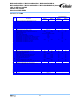
Operating, Standby, and Refresh Currents
T
A
= 0 °C ~ 70 °C; V
DDQ
= V
DD
= 2.5V ± 0.2V (6K); V
DDQ
= V
DD
= 2.6V ± 0.1V (5T)
Symbol
Parameter/Condition Notes
IDD0
Operating Current: one bank; active/precharge; t
RC
= t
RC (MIN)
; t
CK
= t
CK (MIN)
; DQ, DM, and DQS inputs changing twice per
clock cycle; address and control inputs changing once per clock cycle
1,2
IDD1
Operating Current: one bank; active/read/precharge; Burst = 2; t
RC
= t
RC (MIN)
; CL=2.5; t
CK
= t
CK (MIN)
; I
OUT
= 0mA; address and
control inputs changing once per clock cycle
1,2
IDD2P
Precharge Power-Down Standby Current: all banks idle; power-down mode; CKE ≤ V
IL (MAX)
; t
CK
= t
CK (MIN)
1,2
IDD2N
Idle Standby Current: CS ≥ V
IH (MIN)
; all banks idle; CKE ≥ V
IH (MIN)
; t
CK
= t
CK (MIN)
; address and control inputs changing once
per clock cycle
1,2
IDD3P
Active Power-Down Standby Current: one bank active; power-down mode; CKE ≤ V
IL (MAX)
; t
CK
= t
CK (MIN)
1,2
IDD3N
Active Standby Current: one bank; active/precharge; CS ≥ V
IH (MIN)
; CKE ≥ V
IH (MIN)
; t
RC
= t
RAS (MAX)
; t
CK
= t
CK (MIN)
; DQ, DM, and
DQS inputs changing twice per clock cycle; address and control inputs changing once per clock cycle
1,2
IDD4R
Operating Current: one bank; Burst = 2; reads; continuous burst;
address and control inputs changing once per clock cycle;
DQ and DQS outputs changing twice per clock cycle; CL = 2.5; t
CK
= t
CK (MIN)
; I
OUT
= 0mA
1,2
IDD4W
Operating Current: one bank; Burst = 2; writes; continuous burst;
address and control inputs changing once per clock cycle;
DQ and DQS inputs changing twice per clock cycle; CL=2.5; t
CK
= t
CK (MIN)
1,2
IDD5
Auto-Refresh Current: t
RC
= t
RFC (MIN)
1,2,3
IDD6
Self-Refresh Current: CKE ≤ 0.2V 1,2
IDD7
Operating Current: four bank; four bank interleaving with BL = 4, address and control inputs randomly changing; 50% of
data changing at every transfer; t
RC
= t
RC (min)
; I
OUT
= 0mA.
1,2
1. IDD specifications are tested after the device is properly initialized.
2. Input slew rate = 1V/ ns.
3. Current at 7.8 s is time averaged value of IDD5 at t
RFC (MIN)
and IDD2P over 7.8 s.
All IDD current values are calculated from device level.
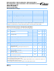
1GB 512MB 256MB
Symbol
(mA)
PC3200
(5T)
PC2700
(6K)
PC3200
(5T)
PC2700
(6K)
PC3200
(5T)
PC2700
(6K)
IDD0
1651 1575 801 765 400 382
mA
IDD1
1702 1634 826 794 413 397
mA
IDD2P
60 57 28 27 14 13
mA
IDD2N
476 420 224 198 112 99
mA
IDD3P
211 195 99 92 50 46
mA
IDD3N
852 767 401 361 200 180
mA
IDD4R
2010 1705 980 830 490 415
mA
IDD4W
2195 1910 1072 932 536 466
mA
IDD5
3225 3125 1587 1540 794 770
mA
IDD6
37 38 17 18 9 9
mA
IDD7
5863 4961 2907 2458 1453 1229
mA