
Datasheet


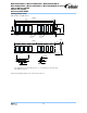


M2U1G64DS8HB1G / M2U51264DS88B1G / M2U25664DSH4B1G
M2Y1G64DS8HB1G / M2Y51264DS88B1G / M2Y25664DSH4B1G (Green)
1GB, 512MB and 256MB
PC3200 and PC2700
Unbuffered DDR DIMM
REV 1.2 11
June 2, 2006
.
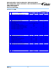
Absolute Maximum Ratings
Symbol Parameter Rating Units
V
IN
, V
OUT
Voltage on I/O pins relative to V
SS
-0.5 to V
DDQ
+0.5 V
V
IN
Voltage on Input relative to V
SS
-0.5 to +3.6 V
V
DD
Voltage on V
DD
supply relative to V
SS
-0.5 to +3.6 V
V
DDQ
Voltage on V
DDQ
supply relative to V
SS
-0.5 to +3.6 V
T
A
Operating Temperature (Ambient) 0 to +70 °C
T
STG
Storage Temperature (Plastic) -55 to +150 °C
P
D
Power Dissipation (per device component)
1 W
I
OUT
Short Circuit Output Current 50 mA
Note: Stresses greater than those listed under “Absolute Maximum Ratings” may cause permanent damage to the device. This is stress
rating only, and functional operation of the device at these or any other conditions above those indicated in the operational secti
ons of this
specification is not implied. Exposure to absolute maximum rating conditions for extended periods may affect reliability.
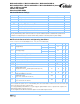
DC Electrical Characteristics and Operating Conditions
T
A
= 0°C ~ 70°C; V
DDQ
= V
DD
= 2.5V±0.2V(6K); T
A
= 0°C ~ 70°C; V
DDQ
= V
DD
= 2.6V±0.1V(5T)
Symbol
Parameter Min Max Units
Notes
6K 2.3
V
DD
Supply Voltage
5T 2.5
2.7 V 1
6K 2.3
V
DDQ
I/O Supply Voltage
5T 2.5
2.7 V 1
V
SS
, V
SSQ
Supply Voltage, I/O Supply Voltage 0 0 V
V
REF
I/O Reference Voltage 0.49 x V
DDQ
0.51 x V
DDQ
V 1, 2
V
TT
I/O Termination Voltage (System) V
REF
– 0.04
V
REF
+ 0.04
V 1, 3
V
IH (DC)
Input High (Logic1) Voltage V
REF
+ 0.15
V
DDQ
+ 0.3
V 1
V
IL (DC)
Input Low (Logic0) Voltage -0.3 V
REF
- 0.15
V 1
V
IN (DC)
Input Voltage Level, CK and Inputs -0.3 V
DDQ
+ 0.3
V 1
V
ID (DC)
Input Differential Voltage, CK and Inputs 0.30 V
DDQ
+ 0.6
V 1, 4
I
I
Input Leakage Current
Any input 0V ≤ VIN ≤ V
DD
; (All other pins not under test = 0V)
-10 10 µA
1
I
OZ
Output Leakage Current
(DQs are disabled; 0V ≤ Vout ≤ V
DDQ
-10 10 µA
1
I
OH
Output High Current
(V
OUT
= V
DDQ
-0.373V, min V
REF
, min V
TT
)
-16.8 - mA
1
I
OL
Output Low Current
(V
OUT
= 0.373, max V
REF
, max V
TT
)
16.8 - mA
1
1. Inputs are not recognized as valid until V
REF
stabilizes.
2. V
REF
is expected to be equal to 0.5 V
DDQ
of the transmitting device, and to track variations in the DC level of the same. Peak-to-peak
noise on V
REF
may not exceed 2% of the DC value.
3. V
TT
is not applied directly to the DIMM. V
TT
is a system supply for signal termination resistors, is expected to be set equal to V
REF
,
and must track variations in the DC level of V
REF
.
4. V
ID
is the magnitude of the difference between the input level on CK and the input level on .