
Datasheet

M2U51264DS8HB3G / M2U25664DS88B3G / M2U12864DSH4B3G
512MB, 256MB and 128MB
PC3200, PC2700 and PC2100
Unbuffered DDR DIMM
REV 2.2 17
Aug 3, 2004
Preliminary
© NANYA TECHNOLOGY CORPORATION
NANYA reserves the right to change products and specifications without notice.
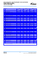
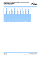
AC Timing Specifications for DDR SDRAM Devices Used on Module
T
A
= 0 °C ~ 70 °C; V
DDQ
= V
DD
= 2.5V ± 0.2V (PC2100/PC2700); V
DDQ
= V
DD
= 2.6V ± 0.1V (PC3200) (Part 2 of 2)
5T
PC3200
6K
PC2700
75B
PC2100
Unit Notes
Symbol Parameter
Min. Max. Min. Max. Min. Max.
t
IS
Address and control input setup time
(slow slew rate)
0.7
0.8 1.0 ns
2-4,
10-12,
14
t
IPW
Input pulse width 2.2 2.2 2.2 ns
2-4, 12
t
RP RE
Read preamble 0.9 1.1 0.9 1.1 0.9 1.1 t
CK
1-4
t
RP ST
Read postamble 0.40 0.60 0.40 0.60 0.40 0.60 t
CK
1-4
t
RAS
Active to Precharge command 42ns 120us 42ns 120us 45ns 120us
1-4
t
RC
Active to Active/Auto-refresh command period 55 60 65 ns
1-4
t
RFC
Auto-refresh to Active/Auto-refresh command
period
70
72 75
ns 1-4
t
RCD
Active to Read or Write delay 15 18 20 ns
1-4
t
RAP
Active to Read Command with Auto-precharge 15 18 20 ns
1-4
t
RP
Precharge command period 15 18 20 ns
1-4
t
RRD
Active bank A to Active bank B command 10 12 15 ns
1-4
t
WR
Write recovery time 15 15 15 ns
1-4
t
DAL
Auto-precharge write recovery + precharge time
(t
WR
/
t
CK
) +
(t
RP
/
t
CK
)
(t
WR
/
t
CK
) +
(t
RP
/
t
CK
)
(t
WR
/
t
CK
) +
(t
RP
/
t
CK
)
t
CK
1-4, 13
t
WTR
Internal write to read command delay 1 1 1 t
CK
1-4
t
PDEX
Power down exit time 5 6 7.5 ns 1-4
t
XSNR
Exit self-refresh to non-read command 75 75 75 ns 1-4
t
XSRD
Exit self-refresh to read command 200 200 200 t
CK
1-4
t
REFI
Average Periodic Refresh Interval 7.8 7.8 7.8 µs 1-4, 8