
Datasheet

M2U51264DS8HB3G / M2U25664DS88B3G / M2U12864DSH4B3G
512MB, 256MB and 128MB
PC3200, PC2700 and PC2100
Unbuffered DDR DIMM
REV 2.2 16
Aug 3, 2004
Preliminary
© NANYA TECHNOLOGY CORPORATION
NANYA reserves the right to change products and specifications without notice.
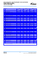
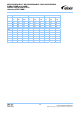
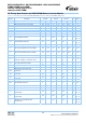
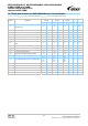
AC Timing Specifications for DDR SDRAM Devices Used on Module
T
A
= 0 °C ~ 70 °C; V
DDQ
= V
DD
= 2.5V ± 0.2V (PC2100/PC2700); V
DDQ
= V
DD
= 2.6V ± 0.1V (PC3200) (Part 1 of 2)
Symbol Parameter
5T
PC3200
6K
PC2700
75B
PC2100
Unit Notes
Min. Max. Min. Max. Min. Max.
t
AC
DQ output access time from CK/CK -0.65 +0.65 -0.7 +0.7 -0.75 +0.75 ns 1-4
t
DQSCK
DQS output access time from CK/CK -0.55 +0.55 -0.7 +0.7 -0.75 +0.75 ns 1-4
t
CH
CK high-level width 0.45 0.55 0.45 0.55 0.45 0.55 t
CK
1-4
t
CL
CK low-level width 0.45 0.55 0.45 0.55 0.45 0.55 t
CK
1-4
t
CK
Clock cycle time CL=3 5 8 - - - -
t
CK
Clock cycle time CL=2.5 6 12 6 12 7.5 12 ns 1-4
t
CK
Clock cycle time CL=2 - - 7.5 12 10 12 ns 1-4
t
DH
DQ and DM input hold time 0.4
0.45 0.5 ns
1-4,
15, 16
t
DS
DQ and DM input setup time 0.4
0.45 0.5 ns
1-4,
15, 16
t
DIPW
DQ and DM input pulse width (each input) 1.75 1.75 1.75 ns 1-4
t
HZ
Data-out high-impedance time from CK/CK -0.6 +0.6 -0.7 +0.7 -0.75 +0.75 ns 1-4, 5
t
LZ
Data-out low-impedance time from CK/CK -0.6 +0.6 -0.7 +0.7 -0.75 +0.75 ns 1-4, 5
t
DQSQ
DQS-DQ skew (DQS & associated DQ signals) 0.4 0.45 0.5 ns 1-4
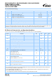
t
HP
Minimum half clk period for any given cycle;
defined by clk high (t
CH
) or clk low (t
CL
) time
t
CH
or
t
CL
t
CH
or
t
CL
t
CH
or
t
CL
t
CK
1-4
t
QH
Data output hold time from DQS
t
HP
-
t
QHS
t
HP
-
t
QHS
t
HP
-
t
QHS
t
CK
1-4
t
QHS
Data hold Skew Factor 0.5 0.55 0.75 ns 1-4
t
DQSS
Write command to 1st DQS latching transition 0.75 1.25 0.75 1.25 0.75 1.25 t
CK
1-4
t
DQSL
,
t
DQSH
DQS input low (high) pulse width
(write cycle)
0.35 0.35 0.35 t
CK
1-4
t
DSS
DQS falling edge to CK setup time
(write cycle)
0.2 0.2 0.2 t
CK
1-4
t
DSH
DQS falling edge hold time from CK
(write cycle)
0.2 0.2 0.2 t
CK
1-4
t
MRD
Mode register set command cycle time 2 2 2 t
CK
1-4
t
WPRES
Write preamble setup time 0 0 0 ns 1-4, 7
t
WPST
Write postamble 0.40 0.60 0.40 0.60 0.40 0.60 t
CK
1-4, 6
t
WPRE
Write preamble 0.25 0.25 0.25 t
CK
1-4
t
IH
Address and control input hold time
(fast slew rate)
0.6
0.75 0.9 ns
2-4, 9,
11, 12
t
IS
Address and control input setup time
(fast slew rate)
0.6
0.75 0.9 ns
2-4, 9,
11, 12
t
IH
Address and control input hold time
(slow slew rate)
0.7
0.8 1.0 ns
2-4,
10, 11,
12, 14