
Datasheet
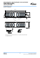
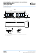

M2U51264DS8HB3G / M2U25664DS88B3G / M2U12864DSH4B3G
512MB, 256MB and 128MB
PC3200, PC2700 and PC2100
Unbuffered DDR DIMM
REV 2.2 14
Aug 3, 2004
Preliminary
© NANYA TECHNOLOGY CORPORATION
NANYA reserves the right to change products and specifications without notice.
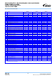
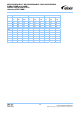
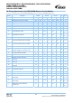
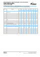
Operating, Standby, and Refresh Currents
T
A
= 0 °C ~ 70 °C; V
DDQ
= V
DD
= 2.5V ± 0.2V (PC2100/PC2700); V
DDQ
= V
DD
= 2.6V ± 0.1V (PC3200)
Symbol Parameter/Condition Notes
IDD0
Operating Current: one bank; active/precharge; t
RC
= t
RC (MIN)
; t
CK
= t
CK (MIN)
; DQ, DM, and DQS inputs changing twice per
clock cycle; address and control inputs changing once per clock cycle
1,2
IDD1
Operating Current: one bank; active/read/precharge; Burst = 2; t
RC
= t
RC (MIN)
; CL=2.5; t
CK
= t
CK (MIN)
; I
OUT
= 0mA; address and
control inputs changing once per clock cycle
1,2
IDD2P
Precharge Power-Down Standby Current: all banks idle; power-down mode; CKE ≤ V
IL (MAX)
; t
CK
= t
CK (MIN)
1,2
IDD2N
Idle Standby Current: CS ≥ V
IH (MIN)
; all banks idle; CKE ≥ V
IH (MIN)
; t
CK
= t
CK (MIN)
; address and control inputs changing once
per clock cycle
1,2
IDD3P
Active Power-Down Standby Current: one bank active; power-down mode; CKE ≤ V
IL (MAX)
; t
CK
= t
CK (MIN)
1,2
IDD3N
Active Standby Current: one bank; active/precharge; CS ≥ V
IH (MIN)
; CKE ≥ V
IH (MIN)
; t
RC
= t
RAS (MAX)
; t
CK
= t
CK (MIN)
; DQ, DM, and
DQS inputs changing twice per clock cycle; address and control inputs changing once per clock cycle
1,2
IDD4R
Operating Current: one bank; Burst = 2; reads; continuous burst; address and control inputs changing once per clock cycle;
DQ and DQS outputs changing twice per clock cycle; CL = 2.5; t
CK
= t
CK (MIN)
; I
OUT
= 0mA
1,2
IDD4W
Operating Current: one bank; Burst = 2; writes; continuous burst; address and control inputs changing once per clock cycle;
DQ and DQS inputs changing twice per clock cycle; CL=2.5; t
CK
= t
CK (MIN)
1,2
IDD5
Auto-Refresh Current: t
RC
= t
RFC (MIN)
1,2,3
IDD6
Self-Refresh Current: CKE ≤ 0.2V 1,2
IDD7
Operating Current: four bank; four bank interleaving with BL = 4, address and control inputs randomly changing; 50% of
data changing at every transfer; t
RC
= t
RC (min)
; I
OUT
= 0mA.
1,2
1. IDD specifications are tested after the device is properly initialized.
2. Input slew rate = 1V/ ns.
3. Current at 7.8 µs is time averaged value of IDD5 at t
RFC (MIN)
and IDD2P over 7.8 µs.
All IDD current values are calculated from device level.