
Datasheet

M2U51264DS8HB3G / M2U25664DS88B3G / M2U12864DSH4B3G
512MB, 256MB and 128MB
PC3200, PC2700 and PC2100
Unbuffered DDR DIMM
REV 2.2 13
Aug 3, 2004
Preliminary
© NANYA TECHNOLOGY CORPORATION
NANYA reserves the right to change products and specifications without notice.
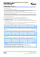
AC Characteristics
Notes 1-5 apply to the following Tables; Electrical Characteristics and DC Operating Conditions, AC Operating
Conditions, Operating, Standby, and Refresh Currents, and Electrical Characteristics and AC Timing.)
1. All voltages referenced to V
SS
.
2. Tests for AC timing, IDD, and electrical, AC and DC characteristics, may be conducted at nominal reference/supply voltage levels, but the
related specifications and device operation are guaranteed for the full voltage range specified.
3. Outputs measured with equivalent load. Refer to the AC Output Load Circuit below.
4. AC timing and IDD tests may use a V
IL
to V
IH
swing of up to 1.5V in the test environment, but input timing is still referenced to V
REF
(or to
the crossing point for CK, CK), and parameter specifications are guaranteed for the specified AC input levels under normal use conditions.
The minimum slew rate for the input signals is 1V/ns in the range between V
IL (AC)
and V
IH (AC)
unless otherwise specified.
5. The AC and DC input level specifications are as defined in the SSTL_2 Standard (i.e. the receiver effectively switches as a result of the
signal crossing the AC input level, and remains in that state as long as the signal does not ring back above (below) the DC input LOW
(HIGH) level.
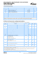
AC Output Load Circuits
Timing Reference Point
V
TT
50 ohms
30 pF
Output
V
OUT
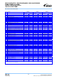
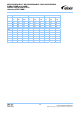
AC Operating Conditions
T
A
= 0 °C ~ 70 °C; V
DDQ
= V
DD
= 2.5V ± 0.2V (PC2100/PC2700); V
DDQ
= V
DD
= 2.6V ± 0.1V (PC3200)
Symbol
Parameter/Condition Min Max Unit Notes
V
IH (AC)
Input High (Logic 1) Voltage. V
REF
+ 0.31 V 1, 2
V
IL (AC)
Input Low (Logic 0) Voltage. V
REF
- 0.31 V 1, 2
V
ID (AC)
Input Differential Voltage, CK and CK Inputs 0.62 V
DDQ
+ 0.6 V 1, 2, 3
V
IX (AC)
Input Differential Pair Cross Point Voltage, CK and CK Inputs (0.5* V
DDQ
) - 0.2 (0.5* V
DDQ
) + 0.2 V 1, 2, 4
1. Input slew rate = 1V/ ns.
2. Inputs are not recognized as valid until V
REF
stabilizes.
3. V
ID
is the magnitude of the difference between the input level on CK and the input level on CK.
4. The value of V
IX
is expected to equal 0.5*V
DDQ
of the transmitting device and must track variations in the DC level of the same.