
Datasheet


M2N1G64TUH8G5F / M2S1G64TUH8G4F / M2N2G64TU8HG5B / M2N2G64TU8HG4B
1GB: 128M x 64 / 2GB: 256M x 64
PC2-5300 / PC2-6400
Unbuffered DDR2 SO-DIMM
REV 1.0 15
07/2010
© NANYA TECHNOLOGY CORPORATION
NANYA reserves the right to change products and specifications without notice.
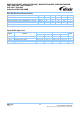
AC Timing Specifications for DDR2 SDRAM Devices Used on Module
(T
CASE
= 0 °C ~ 85 °C; V
DDQ
= 1.8V ± 0.1V; V
DD
= 1.8V ± 0.1V, See AC Characteristics) (Part 1 of 2)
Symbol
Parameter
-3C
-AC
Unit
Notes
Min.
Max.
Min.
Max.
t
AC
DQ output access time from CK/
-0.45
+0.45
-0.40
+0.40
ns
t
DQSCK
DQS output access time from CK/
-0.4
+0.4
-0.35
+0.35
ns
t
CH
CK high-level width
0.48
0.52
0.48
0.52
t
CK
t
CL
CK low-level width
0.48
0.52
0.48
0.52
t
CK
t
HP
Minimum half clk period for any given cycle; defined by clk high
(t
CH
) or clk low (t
CL
) time
Min(tCH(ab.
s),tCL(abs))
-
Min(tCH(ab.
s),tCL(abs))
-
t
CK
t
CK
Clock Cycle Time
3
8
2.5
8
ns
t
DH
DQ and DM input hold time
175
-
125
-
ps
t
DS
DQ and DM input setup time
100
-
50
-
ps
t
IPW
Input pulse width
0.6
-
0.6
-
t
CK
t
DIPW
DQ and DM input pulse width (each input)
0.35
-
0.35
-
t
CK
t
HZ
Data-out high-impedance time from CK/
-
t
AC max
-
t
AC max
ns
t
LZ(DQ)
Data-out low-impedance time from CK/
2xt
AC min
t
AC max
2xt
AC min
t
AC max
ns
t
LZ(DQS)
DQS low-impedance time from CK/
t
AC min
t
AC max
t
AC min
t
AC max
ns
t
DQSQ
DQS-DQ skew (DQS & associated DQ signals)
-
0.24
-
0.20
ns
t
QHS
Data hold Skew Factor
-
0.34
-
0.30
ns
t
QH
Data output hold time from DQS
t
HP
–
t
QHS
-
t
HP
–
t
QHS
-
ns
t
DQSS
Write command to 1
st
DQS latching transition
-0.25
0.25
-0.25
0.25
t
CK
t
DQSH
DQS input high pulse width
0.35
-
0.35
-
t
CK
t
DQSL
DQS input low pulse width
0.35
-
0.35
-
t
CK
t
DSS
DQS falling edge to CK setup time
(write cycle)
0.2
-
0.2
-
t
CK
t
DSH
DQS falling edge hold time from CK
(write cycle)
0.2
-
0.2
-
t
CK
t
MRD
Mode register set command cycle time
2
-
2
-
t
CK
t
WPST
Write postamble
0.40
0.60
0.40
0.60
t
CK
t
WPRE
Write preamble
0.35
-
0.35
-
t
CK
t
IH
Address and control input hold time
0.275
-
0.250
-
ns
t
IS
Address and control input setup time
0.2
-
0.175
-
ns
t
RPRE
Read preamble
0.9
1.1
0.9
1.1
t
CK
t
RPST
Read postamble
0.4
0.6
0.4
0.6
t
CK
t
Delay
Minimum time clocks remains ON after CKE asynchronously
drops Low
t
IS
+ t
CK(avg)
+
t
IH
-
t
IS
+ t
CK(avg)
+
t
IH
-
ns
t
RFC
Refresh to active/Refresh command time
127.5
127.5
ns
t
REFI
Average Periodic Refresh Interval
(85ºC < T
CASE
≤ 95ºC)
3.9
3.9
μs
Average Periodic Refresh Interval
(0ºC ≤ T
CASE
≤ 85ºC)
7.8
7.8
μs