
Datasheet


M2N1G64TUH8G5F / M2S1G64TUH8G4F / M2N2G64TU8HG5B / M2N2G64TU8HG4B
1GB: 128M x 64 / 2GB: 256M x 64
PC2-5300 / PC2-6400
Unbuffered DDR2 SO-DIMM
REV 1.0 13
07/2010
© NANYA TECHNOLOGY CORPORATION
NANYA reserves the right to change products and specifications without notice.
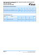
Operating, Standby, and Refresh Currents
T
CASE
= 0 °C ~ 85 °C; V
DDQ
= V
DD
= 1.8V ± 0.1V [1GB, 2 Ranks, 64Mx16 DDR2 SDRAMs]
Symbol
Parameter/Condition
PC2-5300
(-3C)
PC2-6400
(-AC)
Unit
IDD0
Operating Current: one bank; active/precharge; t
RC
= t
RC (MIN)
; t
CK
= t
CK
(MIN)
; DQ, DM, and DQS inputs changing twice per clock cycle; address
and control inputs changing once per clock cycle
660
792
mA
IDD1
Operating Current: one bank; active/read/precharge; Burst = 4; t
RC
= t
RC
(MIN)
; CL= 4; t
CK
= t
CK (MIN)
; I
OUT
= 0mA; address and control inputs
changing once per clock cycle
748
858
mA
IDD2P
Precharge Power-Down Standby Current: all banks idle; power-down
mode; CKE V
IL (MAX)
; t
CK
= t
CK (MIN)
79
79
mA
IDD2Q
Precharge quiet standby current
440
528
mA
IDD2N
Idle Standby Current: CS V
IH (MIN)
; all banks idle; CKE V
IH (MIN)
; t
CK
= t
CK
(MIN)
; address and control inputs changing once per clock cycle
440
572
mA
IDD3N
Active Standby Current: one bank; active/precharge; CS V
IH (MIN)
; CKE
V
IH (MIN)
; t
RC
= t
RAS (MAX)
; t
CK
= t
CK (MIN)
; DQ, DM, and DQS inputs changing
twice per clock cycle; address and control inputs changing once per
clock cycle
506
616
mA
IDD4R
Operating Current: one bank; Burst = 4; reads; continuous burst;
address and control inputs changing once per clock cycle; DQ and DQS
outputs changing twice per clock cycle; CL = 4; t
CK
= t
CK (MIN)
; I
OUT
= 0mA
880
1320
mA
IDD4W
Operating Current: one bank; Burst = 4; writes; continuous burst;
address and control inputs changing once per clock cycle; DQ and DQS
inputs changing twice per clock cycle; CL= 4; t
CK
= t
CK (MIN)
880
1320
mA
IDD5B
Burst Refresh Current: t
RC
= t
RFC (MIN)
1100
1210
mA
IDD6
Self-Refresh Current: CKE 0.2V
79
79
mA
IDD7
Operating Current: four bank; four bank interleaving with BL = 4,
address and control inputs randomly changing; 50% of data changing at
every transfer; t
RC
= t
RC (min)
; I
OUT
= 0mA.
1364
1738
mA
Note: Module IDD was calculated from component IDD. It may differ from the actual measurement.