
User's Manual Part 2
The M.2 modules utilize a single regulated power rail of 3.3 V provided by the host
platform. There is no other VDDIO like pin and the M.2 module is responsible for
generating its own I/O voltage source using the 3.3 V power rail. This
3.3 V voltage rail source on the platform should always be on and available during the
system’s stand-by/suspend state to support the wake event processing on the
communications card.
There are 5 power pins on the host interface, pins 2, 4, 70, 72, and 74.
The requirements of the regulated 3.3 V power supply provided by the host platform are
listed below.
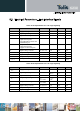
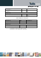
Table 25 M.2 Module Power Delivery Requirements - Ultrabook
Requirement Detailed Description
Supply voltage 3.3 V at the Card connector will be within 5% tolerance on the
motherboard.
Peak Current The host board shall provide 2.5 A peak current.
Average Current Average max current of 1.1 A will be supported.
Max in-rush current Max module in-rush current of 5.1 A will be supported.
Power pin
connections
The power pins specified in WWAN card #’s, 2, 4, 70, 72, 74 will be connected
to 3.3 V supply and WWAN configuration pins 1, 69, and 75 will be connected
to ground.
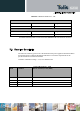
For Tablet platforms, the 3.3 V regulated power rail can be replaced with a direct VBAT
connection. Key parameters for VBAT in a direct connection configuration are shown in
Table 26.
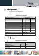
Table 26 VBAT Power Delivery Requirements – Direct Connections (Tablet)
Power Source Vmin Vmax Cell Type
VBAT 3.135 V* 4.4 V Once cell Li-Ion battery
(*) RF performance cannot be guaranteed below 3.135 V.