
Manual


-58-
T
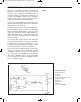
ry to mark 0 and 1 inputs on the schematic and see
if this circuit comes up at either a 0 or 1 output. Give
it try and don’t peak at the answer.
As you are constructing this circuit, make sure to
have the switch set to B. Once you have completed
the wiring, connect to terminals 13 and 14. Now
press the key. Are there any changes in LED 1?
Now release the key and place the switch to A. Now
what occurs on LED 1? Leave the switch at A and
then press the key. Is anything different occurring?
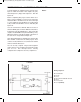
This project acts just like the other NOR gates we
have built. The NANDs mark with an A and B both
have an input of 1. Therefore they both have an
output of 0 when the input is 1. Their outputs are
used as inputs to the NAND labeled C. The output
of NAND C is 1 as long as one or both of inputs are
0. This output is used for the inputs of the next
NAND causing it to have an output of 0. Therefore
the LED 1 does not light.
A NOR gate only has an output of 1 when both
inputs are 0. This occurs when the switch is set to B
and the key is not pressed.
N
otes:
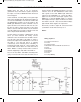
EXPERIMENT #42: “NOR” GATE USING TTL
Wiring Sequence:
o 13-49-131-137
o 14-119
o 31-55
o 72-33-62-133-121
o 50-58
o 51-61
o 52-53-54
o 56-57-71-138
o 59-60-132
o 13-14 (POWER)
Schematic
EP-130_62315RevC.qxp_EP-130_062812 6/23/15 11:17 AM Page 58