
Manual


-53-
One of the cool things about the quad two-input
N
AND IC is that to make up other logic circuits all
we have to do is combine the four NAND gates. In
our last two projects you have been shown how you
are able to use NANDs to make up some other logic
circuits. In this project you will be shown how to
make up an OR gate from the NAND gates.
Can you trace what happens from each input to the
eventual output from just looking at the schematic?
(Of course you can, just try it.)
Keep the switch set to B, as you work on this project.
Connect terminals 13 and 14 when you’ve finished.
Now press the key. What happens to LED 1? Set the
switch to A and release the key. What happens to
LED 1 now? Press the key again while keeping the
switch at A and press the key again. Are there any
changes in LED 1?
You see that this circuit acts like other OR gates
you’ve experimented with. The output to the LED is
1 if at least one or the other of the inputs is 1. Have
you tried tracing what happens from input to output
yet? The explanation is in the next paragraph.
Say you press the key with the switch set to B. This
enters 1 as both inputs of the NAND, thus causing
the NAND’s output to become 0. This 0 output is
one of the inputs to the NAND gate controlling the
LED. Since a NAND’s output is 0 only if all inputs
are 1, then the 0 input causes the NAND’s output to
go to 1, and LED 1 lights!
Notes:
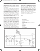
EXPERIMENT #37: “OR” GATE USING TTL
Wiring Sequence:
o 13-49-131-137
o 14-119
o 31-58
o 72-59-60-62-33-133-121
o 50-51-71-138
o 52-56
o 53-54-132
o 55-57
o 13-14 (POWER)
Schematic
EP-130_62315RevC.qxp_EP-130_062812 6/23/15 11:17 AM Page 53