
User Manual


© EA Elektro-Automatik GmbH & Co. KG, DE-41747 Viersen, Helmholtzstr. 31-33, Tel. 02162-3785-0, Fax. 02162-16230
7
Technical description
General
The laboratory power supply series PS 3000 B is an ideal equipment for the use in R&D , schools (vocational training), maintenance
and production. The attractive design, the easy and intuitive handling and the rugged and reliable technology make this series an
ideal tool for technicians, engineers and their apprentices.
Adjustment of the output
Output voltage and output current can be set from 0 up to the max. value. Both operation modes, constant voltage (CV) or constant
current (CV), are selected automatically (auto crossover).
Load connection
The load can be connected through the safety sockets on the front or via screw terminals on the rear side.
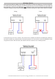
Remote sense
The output voltage loss resulting from long DC output cables can be compensated by connecting the sense terminal (+ and – sense)
on the rear side with the + and – input terminals of the load. For this purpose please remove the jumpers from the terminals + Sense
and – Sense rstly.
Overvoltage protection (OVP)
The units are equipped with an overvoltage protection (OVP). The value can be adjusted with a screw driver between 0V...110% of
the rated output voltage. If the output voltage becomes higher than the preset value, due to a user’s mistake or an internal defect, the
output will shut down and the LED OVP will light up.
Fan control and overtemperature protection (OT)
The series is equipped with a temperature regulated fan speed. In case the temperature of the transformer or the power stage be-
comes too high, the output is switched off automatically. The LED OT (overtemperature) will light up. After cooling down the unit will
reset automatically.
Interfacing
The built-in analog interface allows to control the unit externally through analog signals (0-10 V). With the external, optional interface
UTA12 it is possible to control the unit via a personal computer. The software for this application (UTA12) is provided.
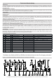
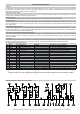
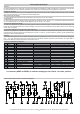
Pin assignment of analog interface
Internal schematic diagram analog interface
The grounds of the unit (AGND and DGND) are electrically connected to the positive output!
Pin Name I/O Description Phasing Description, level, impedance
1 VSEL I Nominal value voltage - 0…10V, input impedance >40kΩ
2 CSEL I Nominal value current - 0…10V, input impedance >40kΩ
3 VREF O Reference value - 10V, I
Max
= 5mA
4 DGND - Digital Ground - Ground for control and status signals
5 SEL-enable I Select local / extern Low=Extern Open=Local U
Max
= 20V, I
Max
= 2mA, U
Low
<1V
6 OT O Overtemperature Low=OK Open=Error U
Max
= 20V, I
Max
= -25mA, open collector
7 NC - - -
8 NC - - -
9 VMON O Actual value voltage 0...10V, I
Max
= 2mA
10 CMON O Actual value current 0...10V, I
Max
= 2mA
11 AGND - Analog Ground Ground nominal and actual values, VREF
12 +VCC O Supply voltage 11...15V, I
Max
= 100mA
13 Standby I Output on / off Low=Off Open=On U
Max
= 20V, I
Max
= 2mA, U
Low
<1V
14 OVP O Overvoltage Low=OK Open=Error U
Max
= 20V, I
Max
= -25mA, open collector
15 CV/CC O Voltage or current control Low=CV Open=CC U
Max
= 20V, I
Max
= -25mA, open collector
I = input, O = output