
Data Sheet

PN512_C1_SDS All information provided in this document is subject to legal disclaimers. © NXP B.V. 2012. All rights reserved.
Product short data sheet
COMPANY PUBLIC
Rev. 3.2 — 20 September 2012
120132 8 of 27
NXP Semiconductors
PN532/C1
Near Field Communication (NFC) controller
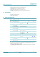
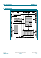
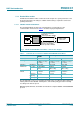
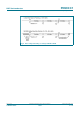
7.1.2 Simplified block diagram
The Analog Interface handles the modulation and demodulation of the analog signals
according to the Card emulation mode, Reader/Writer mode and NFCIP-1 mode
communication scheme.
The RF level detector detects the presence of an external RF-field delivered by the
antenna to the RX pin.
The data mode detector detects a ISO/IEC 14443-A MIFARE, FeliCa or NFCIP-1 mode in
order to prepare the internal receiver to demodulate signals, which are sent to the PN532.
The NFC-WI/S
2
C interface supports communication to secure IC. It also supports digital
signals for transfer speeds above 424 kbit/s.
The CL UART handles the protocol requirements for the communication schemes in
co-operation with the appropriate firmware. The FIFO buffer allows a convenient data
transfer from the 80C51 to the CIU and vice versa.
Fig 2. Simplify Contactless Interface Unit (CIU) block diagram
80C51
FIFO
Serial
CL UARTData
Switch
Data
RF
Mode
Detector
Level
Detector
Analog
Interface
Antenna
PN532
Contactless Interface Unit