
Data Sheet

DS3231 I
2
C interface may be placed into a known state
by toggling SCL until SDA is observed to be at a high
level. At that point the microcontroller should pull SDA
low while SCL is high, generating a START condition.
Clock and Calendar
The time and calendar information is obtained by read-
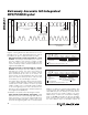
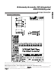
ing the appropriate register bytes. Figure 1 illustrates the
RTC registers. The time and calendar data are set or ini-
tialized by writing the appropriate register bytes. The con-
tents of the time and calendar registers are in the
binary-coded decimal (BCD) format. The DS3231 can be
run in either 12-hour or 24-hour mode. Bit 6 of the hours
register is defined as the 12- or 24-hour mode select bit.
When high, the 12-hour mode is selected. In the 12-hour
mode, bit 5 is the AM/PM bit with logic-high being PM. In
the 24-hour mode, bit 5 is the second 10-hour bit (20–23
hours). The century bit (bit 7 of the month register) is tog-
gled when the years register overflows from 99 to 00.
The day-of-week register increments at midnight.
Values that correspond to the day of week are user-
defined but must be sequential (i.e., if 1 equals
Sunday, then 2 equals Monday, and so on). Illogical
time and date entries result in undefined operation.
When reading or writing the time and date registers, sec-
ondary (user) buffers are used to prevent errors when
the internal registers update. When reading the time and
date registers, the user buffers are synchronized to the
internal registers on any START and when the register
pointer rolls over to zero. The time information is read
from these secondary registers, while the clock contin-
ues to run. This eliminates the need to reread the regis-
ters in case the main registers update during a read.
DS3231
Extremely Accurate I
2
C-Integrated
RTC/TCXO/Crystal
____________________________________________________________________ 11
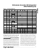
Figure 1. Timekeeing Registers
Note: Unless otherwise specified, the registers’ state is not defined when power is first applied.
ADDRESS
BIT 7
MSB
BIT 6
BIT 5
BIT 4 BIT 3
BIT 2
BIT 1
BIT 0
LSB
FUNCTION RANGE
00H 0 10 Seconds Seconds Seconds 00–59
01H 0 10 Minutes Minutes Minutes 00–59
AM/PM
02H 0
12/24
10 Hour
10 Hour
Hour Hours
1–12 + AM/PM
00–23
03H 0 0 0 0 0 Day Day 1–7
04H 0 0 10 Date Date Date 00–31
05H
Century
00
10 Month
Month
Month/
Century
01–12 +
Century
06H 10 Year Year Year 00–99
07H
A1M1
10 Seconds Seconds
Alarm 1 Seconds
00–59
08H
A1M2
10 Minutes Minutes
Alarm 1 Minutes
00–59
AM/PM
09H
A1M3 12/24
10 Hour
10 Hour
Hour
Alarm 1 Hours
1–12 + AM/PM
00–23
Day Alarm 1 Day 1–7
0AH
A1M4 DY/DT
10 Date
Date Alarm 1 Date 1–31
0BH
A2M2
10 Minutes Minutes
Alarm 2 Minutes
00–59
AM/PM
0CH
A2M3 12/24
10 Hour
10 Hour
Hour
Alarm 2 Hours
1–12 + AM/PM
00–23
Day Alarm 2 Day 1–7
0DH
A2M4 DY/DT
10 Date
Date Alarm 2 Date 1–31
0EH
EOSC BBSQW CONV
RS2 RS1
INTCN A2IE A1IE
Control —
0FH
OSF
00 0
EN32kHz BSY A2F A1F
Control/Status —
10H
SIGN DATA DATA DATA
DATA
DATA DATA DATA
Aging Offset —
11H
SIGN DATA DATA DATA
DATA
DATA DATA DATA
MSB of Temp —
12H
DATA
DATA
00 0000LSB of Temp —