
Data Sheet


CC1101
SWRS061B Page 88 of 93
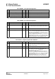
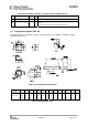
34.1 Recommended PCB Layout for Package (QLP 20)
Figure 31: Recommended PCB Layout for QLP 20 Package
Note: Figure 31 is an illustration only and not to scale. There are five 10 mil via holes distributed
symmetrically in the ground pad under the package. See also the CC1101EM reference designs
([5] and [6]).
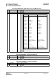
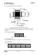
34.2 Package Thermal Properties
Thermal Resistance
Air velocity [m/s] 0
Rth,j-a [K/W] 40.4
Table 39: Thermal Properties of QLP 20 Package
34.3 Soldering Information
The recommendations for lead-free reflow in IPC/JEDEC J-STD-020C should be followed.
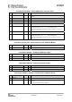
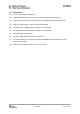
34.4 Tray Specification
CC1101
can be delivered in standard QLP 4x4 mm shipping trays.
Tray Specification
Package Tray Width Tray Height Tray Length Units per Tray
QLP 20 135.9mm 7.62mm 322.6mm 490
Table 40: Tray Specification