
Data Sheet


CC1101
SWRS061B Page 84 of 93
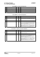
33.3 Status Register Details
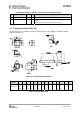
0x30 (0xF0): PARTNUM – Chip ID
Bit Field Name Reset R/W Description
7:0 PARTNUM[7:0] 0 (0x00) R Chip part number
0x31 (0xF1): VERSION – Chip ID
Bit Field Name Reset R/W Description
7:0 VERSION[7:0] 4 (0x04) R Chip version number.
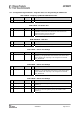
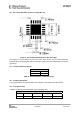
0x32 (0xF2): FREQEST – Frequency Offset Estimate from Demodulator
Bit Field Name Reset R/W Description
7:0 FREQOFF_EST R The estimated frequency offset (2’s complement) of the carrier. Resolution is
F
XTAL
/2
14
(1.59 - 1.65 kHz); range is ±202 kHz to ±210 kHz, dependent of XTAL
frequency.
Frequency offset compensation is only supported for 2-FSK, GFSK, and MSK
modulation. This register will read 0 when using ASK or OOK modulation.
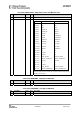
0x33 (0xF3): LQI – Demodulator Estimate for Link Quality
Bit Field Name Reset R/W Description
7 CRC OK R The last CRC comparison matched. Cleared when entering/restarting RX
mode.
6:0 LQI_EST[6:0] R The Link Quality Indicator estimates how easily a received signal can be
demodulated. Calculated over the 64 symbols following the sync word
0x34 (0xF4): RSSI – Received Signal Strength Indication
Bit Field Name Reset R/W Description
7:0 RSSI R Received signal strength indicator