
Data Sheet


CC1101
SWRS061B Page 80 of 93
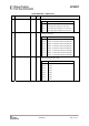
0x1F: WOREVT0 –Low Byte Event0 Timeout
Bit Field Name Reset R/W Description
7:0 EVENT0[7:0] 107 (0x6B) R/W
Low byte of EVENT0 timeout register.
The default EVENT0 value gives 1.0s timeout, assuming a 26.0 MHz
crystal.
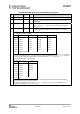
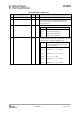
0x20: WORCTRL – Wake On Radio Control
Bit Field Name Reset R/W Description
7 RC_PD 1 R/W Power down signal to RC oscillator. When written to 0, automatic initial
calibration will be performed
6:4 EVENT1[2:0] 7 (111) R/W Timeout setting from register block. Decoded to Event 1 timeout. RC
oscillator clock frequency equals F
XOSC
/750, which is 34.7 – 36 kHz,
depending on crystal frequency. The table below lists the number of clock
periods after Event 0 before Event 1 times out.
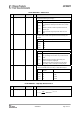
Setting t
Event1
0 (000) 4 (0.111 – 0.115 ms)
1 (001) 6 (0.167 – 0.173 ms)
2 (010) 8 (0.222 – 0.230 ms)
3 (011) 12 (0.333 – 0.346 ms)
4 (100) 16 (0.444 – 0.462 ms)
5 (101) 24 (0.667 – 0.692 ms)
6 (110) 32 (0.889 – 0.923 ms)
7 (111) 48 (1.333 – 1.385 ms)
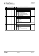
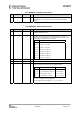
3 RC_CAL 1 R/W Enables (1) or disables (0) the RC oscillator calibration.
2 Reserved R0
1:0 WOR_RES 0 (00) R/W Controls the Event 0 resolution as well as maximum timeout of the WOR
module and maximum timeout under normal RX operation::
Setting Resolution (1 LSB) Max timeout
0 (00) 1 period (28µs – 29µs) 1.8 – 1.9 seconds
1 (01) 2
5
periods (0.89ms –0.92 ms) 58 – 61 seconds
2 (10) 2
10
periods (28 – 30 ms) 31 – 32 minutes
3 (11) 2
15
periods (0.91 – 0.94 s) 16.5 – 17.2 hours
Note that WOR_RES should be 0 or 1 when using WOR because
WOR_RES > 1 will give a very low duty cycle.
In normal RX operation all settings of WOR_RES can be used.