
Data Sheet


CC1101
SWRS061B Page 7 of 93
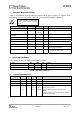
1 Absolute Maximum Ratings
Under no circumstances must the absolute maximum ratings given in Table 1 be violated. Stress
exceeding one or more of the limiting values may cause permanent damage to the device.
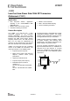
Caution! ESD sensitive device.
Precaution should be used when handling
the device in order to prevent permanent
damage.
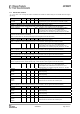
Parameter Min Max Units Condition
Supply voltage –0.3 3.9 V All supply pins must have the same voltage
Voltage on any digital pin –0.3 VDD + 0.3
max 3.9
V
Voltage on the pins RF_P, RF_N,
and DCOUPL
–0.3 2.0 V
Voltage ramp-up rate 120 kV/µs
Input RF level +10 dBm
Storage temperature range –50 150
°C
Solder reflow temperature 260
°C
According to IPC/JEDEC J-STD-020C
ESD 750 V According to JEDEC STD 22, method A114,
Human Body Model (HBM)
ESD 400 V According to JEDEC STD 22, C101C,
Charged Device Model (CDM)
Table 1: Absolute Maximum Ratings
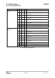
2 Operating Conditions
The operating conditions for
CC1101
are listed Table 2 in below.
Parameter Min Max Unit Condition
Operating temperature -40 85
°C
Operating supply voltage 1.8 3.6 V All supply pins must have the same voltage
Table 2: Operating Conditions
3 General Characteristics
Parameter Min Typ Max Unit Condition/Note
Frequency range 300 348 MHz
387 464 MHz
779 928 MHz
Data rate 1.2
1.2
26
500
250
500
kBaud
kBaud
kBaud
2-FSK
GFSK, OOK, and ASK
(Shaped) MSK (also known as differential offset
QPSK)
Optional Manchester encoding (the data rate in kbps
will be half the baud rate)
Table 3: General Characteristics