
Data Sheet


CC1101
SWRS061B Page 63 of 93
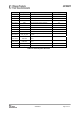
Table 37: SPI Address Space
33.1 Configuration Register Details – Registers with preserved values in SLEEP state
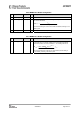
0x00: IOCFG2 – GDO2 Output Pin Configuration
Bit Field Name Reset R/W Description
7 Reserved R0
6
GDO2
_INV
0 R/W Invert output, i.e. select active low (1) / high (0)
5:0
GDO2
_CFG[5:0]
41 (0x29) R/W
Default is CHP_RDYn (See Table 33 on page 55).
0x01: IOCFG1 – GDO1 Output Pin Configuration
Bit Field Name Reset R/W Description
7 GDO_DS 0 R/W Set high (1) or low (0) output drive strength on the GDO pins.
6
GDO1
_INV
0 R/W Invert output, i.e. select active low (1) / high (0)
5:0
GDO1
_CFG[5:0]
46 (0x2E) R/W Default is 3-state (See Table 33 on page 55).
0x02: IOCFG0 – GDO0 Output Pin Configuration
Bit Field Name Reset R/W Description
7 TEMP_SENSOR_ENABLE 0 R/W Enable analog temperature sensor. Write 0 in all other register
bits when using temperature sensor.
6
GDO0
_INV
0 R/W Invert output, i.e. select active low (1) / high (0)
5:0
GDO0
_CFG[5:0]
63 (0x3F) R/W Default is CLK_XOSC/192 (See Table 33 on page 55).
It is recommended to disable the clock output in initialization,
in order to optimize RF performance.