
Data Sheet


CC1101
SWRS061B Page 57 of 93
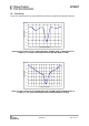
32.2 Frequency Hopping and Multi-
Channel Systems
The 433 MHz, 868 MHz, or 915 MHz bands
are shared by many systems both in industrial,
office, and home environments. It is therefore
recommended to use frequency hopping
spread spectrum (FHSS) or a multi-channel
protocol because the frequency diversity
makes the system more robust with respect to
interference from other systems operating in
the same frequency band. FHSS also combats
multipath fading.
CC1101
is highly suited for FHSS or multi-
channel systems due to its agile frequency
synthesizer and effective communication
interface. Using the packet handling support
and data buffering is also beneficial in such
systems as these features will significantly
offload the host controller.
Charge pump current, VCO current, and VCO
capacitance array calibration data is required
for each frequency when implementing
frequency hopping for
CC1101
. There are 3
ways of obtaining the calibration data from the
chip:
1) Frequency hopping with calibration for each
hop. The PLL calibration time is approximately
720 µs. The blanking interval between each
frequency hop is then approximately 810 us.
2) Fast frequency hopping without calibration
for each hop can be done by calibrating each
frequency at startup and saving the resulting
FSCAL3, FSCAL2, and FSCAL1 register values
in MCU memory. Between each frequency
hop, the calibration process can then be
replaced by writing the FSCAL3, FSCAL2and
FSCAL1 register values corresponding to the
next RF frequency. The PLL turn on time is
approximately 90 µs. The blanking interval
between each frequency hop is then
approximately 90 us. The VCO current
calibration result available in FSCAL2 is not
dependent on the RF frequency. Neither is the
charge pump current calibration result
available in FSCAL3. The same value can
therefore be used for all frequencies.
3) Run calibration on a single frequency at
startup. Next write 0 to FSCAL3[5:4] to
disable the charge pump calibration. After
writing to FSCAL3[5:4] strobe SRX (or STX)
with MCSM0.FS_AUTOCAL=1 for each new
frequency hop. That is, VCO current and VCO
capacitance calibration is done but not charge
pump current calibration. When charge pump
current calibration is disabled the calibration
time is reduced from approximately 720 µs to
approximately 150 µs. The blanking interval
between each frequency hop is then
approximately 240 us.
There is a trade off between blanking time and
memory space needed for storing calibration
data in non-volatile memory. Solution 2) above
gives the shortest blanking interval, but
requires more memory space to store
calibration values. Solution 3) gives
approximately 570 µs smaller blanking interval
than solution 1).
Note that the recommended settings for
TEST0.VCO_SEL_CAL_EN will change with
frequency. This means that one should always
use SmartRF
®
Studio [7] to get the correct
settings for a specific frequency before doing a
calibration, regardless of which calibration
method is being used.
It must be noted that the TESTn registers (n =
0, 1, or 2) content is not retained in SLEEP
state, and thus it is necessary to re-write these
registers when returning from the SLEEP
state.
32.3 Wideband Modulation not using
Spread Spectrum
Digital modulation systems under FFC part
15.247 includes 2-FSK and GFSK modulation.
A maximum peak output power of 1W (+30
dBm) is allowed if the 6 dB bandwidth of the
modulated signal exceeds 500 kHz. In
addition, the peak power spectral density
conducted to the antenna shall not be greater
than +8 dBm in any 3 kHz band.
Operating at high data rates and frequency
separation, the
CC1101
is suited for systems
targeting compliance with digital modulation
system as defined by FFC part 15.247. An
external power amplifier is needed to increase
the output above +10 dBm.
32.4 Data Burst Transmissions
The high maximum data rate of
CC1101
opens
up for burst transmissions. A low average data
rate link (e.g. 10 kBaud), can be realized using
a higher over-the-air data rate. Buffering the
data and transmitting in bursts at high data
rate (e.g. 500 kBaud) will reduce the time in
active mode, and hence also reduce the
average current consumption significantly.
Reducing the time in active mode will reduce
the likelihood of collisions with other systems
in the same frequency range.