
Data Sheet


CC1101
SWRS061B Page 56 of 93
31 Asynchronous and Synchronous Serial Operation
Several features and modes of operation have
been included in the
CC1101
to provide
backward compatibility with previous Chipcon
products and other existing RF communication
systems. For new systems, it is recommended
to use the built-in packet handling features, as
they can give more robust communication,
significantly offload the microcontroller, and
simplify software development.
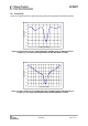
31.1 Asynchronous Operation
For backward compatibility with systems
already using the asynchronous data transfer
from other Chipcon products, asynchronous
transfer is also included in
CC1101
. When
asynchronous transfer is enabled, several of
the support mechanisms for the MCU that are
included in
CC1101
will be disabled, such as
packet handling hardware, buffering in the
FIFO, and so on. The asynchronous transfer
mode does not allow the use of the data
whitener, interleaver, and FEC, and it is not
possible to use Manchester encoding.
Note that MSK is not supported for
asynchronous transfer.
Setting PKTCTRL0.PKT_FORMAT to 3
enables asynchronous serial mode.
In TX, the GDO0 pin is used for data input (TX
data). Data output can be on GDO0, GDO1, or
GDO2. This is set by the IOCFG0.GDO0_CFG,
IOCFG1.GDO1_CFG and IOCFG2.GDO2_CFG
fields.
The
CC1101
modulator samples the level of the
asynchronous input 8 times faster than the
programmed data rate. The timing requirement
for the asynchronous stream is that the error in
the bit period must be less than one eighth of
the programmed data rate.
31.2 Synchronous Serial Operation
Setting PKTCTRL0.PKT_FORMAT to 1
enables synchronous serial mode. In the
synchronous serial mode, data is transferred
on a two wire serial interface. The
CC1101
provides a clock that is used to set up new
data on the data input line or sample data on
the data output line. Data input (TX data) is the
GDO0 pin. This pin will automatically be
configured as an input when TX is active. The
data output pin can be any of the GDO pins;
this is set by the IOCFG0.GDO0_CFG,
IOCFG1.GDO1_CFG, and IOCFG2.GDO2_CFG
fields.
Preamble and sync word insertion/detection
may or may not be active, dependent on the
sync mode set by the MDMCFG2.SYNC_MODE.
If preamble and sync word is disabled, all
other packet handler features and FEC should
also be disabled. The MCU must then handle
preamble and sync word insertion and
detection in software. If preamble and sync
word insertion/detection is left on, all packet
handling features and FEC can be used. One
exception is that the address filtering feature is
unavailable in synchronous serial mode.
When using the packet handling features in
synchronous serial mode, the
CC1101
will insert
and detect the preamble and sync word and
the MCU will only provide/get the data
payload. This is equivalent to the
recommended FIFO operation mode.
32 System Considerations and Guidelines
32.1 SRD Regulations
International regulations and national laws
regulate the use of radio receivers and
transmitters. Short Range Devices (SRDs) for
license free operation below 1 GHz are usually
operated in the 433 MHz, 868 MHz or 915
MHz frequency bands. The
CC1101
is
specifically designed for such use with its 300 -
348 MHz, 387 - 464 MHz, and 779 - 928 MHz
operating ranges. The most important
regulations when using the
CC1101
in the 433
MHz, 868 MHz, or 915 MHz frequency bands
are EN 300 220 (Europe) and FCC CFR47
part 15 (USA). A summary of the most
important aspects of these regulations can be
found in Application Note AN001 [2].
Please note that compliance with regulations is
dependent on complete system performance.
It is the customer’s responsibility to ensure that
the system complies with regulations.