
Data Sheet


CC1101
SWRS061B Page 54 of 93
separate via. Direct connections between
neighboring power pins will increase noise
coupling and should be avoided unless
absolutely necessary.
The external components should ideally be as
small as possible (0402 is recommended) and
surface mount devices are highly
recommended. Please note that components
smaller than those specified may have
differing characteristics.
Precaution should be used when placing the
microcontroller in order to avoid noise
interfering with the RF circuitry.
A CC1101DK Development Kit with a fully
assembled CC1101EM Evaluation Module is
available. It is strongly advised that this
reference layout is followed very closely in
order to get the best performance. The
schematic, BOM and layout Gerber files are all
available from the TI website ([5] and [6]).
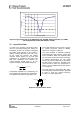
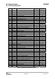
Figure 28: Left: Top Solder Resist Mask (Negative). Right: Top Paste Mask. Circles are Vias
30 General Purpose / Test Output Control Pins
The three digital output pins GDO0, GDO1,
and GDO2 are general control pins configured
with IOCFG0.GDO0_CFG,
IOCFG1.GDO1_CFG, and IOCFG2.GDO3_CFG
respectively. Table 33 shows the different
signals that can be monitored on the GDO
pins. These signals can be used as inputs to
the MCU. GDO1 is the same pin as the SO pin
on the SPI interface, thus the output
programmed on this pin will only be valid when
CSn is high. The default value for GDO1 is 3-
stated, which is useful when the SPI interface
is shared with other devices.
The default value for GDO0 is a 135-141 kHz
clock output (XOSC frequency divided by
192). Since the XOSC is turned on at power-
on-reset, this can be used to clock the MCU in
systems with only one crystal. When the MCU
is up and running, it can change the clock
frequency by writing to IOCFG0.GDO0_CFG.
An on-chip analog temperature sensor is
enabled by writing the value 128 (0x80) to the
IOCFG0 register. The voltage on the GDO0
pin is then proportional to temperature. See
Section 4.7 on page 15 for temperature sensor
specifications.
If the IOCFGx.GDOx_CFG setting is less than
0x20 and IOCFGx_GDOx_INV is 0 (1), the
GDO0 and GDO2 pins will be hardwired to 0
(1) and the GDO1 pin will be hardwired to 1
(0) in the SLEEP state. These signals will be
hardwired until the CHIP_RDYn signal goes
low.
If the IOCFGx.GDOx_CFG setting is 0x20 or
higher the GDO pins will work as programmed
also in SLEEP state. As an example, GDO1 is
high impedance in all states if
IOCFG1.GDO1_CFG=0x2E.